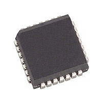
MC10E195FNG ON Semiconductor, MC10E195FNG Datasheet - Page 6

MC10E195FNG
Manufacturer Part Number
MC10E195FNG
Description
IC PROGRAM DELAY ECL 5V 28PLCC
Manufacturer
ON Semiconductor
Series
10Er
Type
Programmable Delay Chipr
Datasheet
1.MC100E195FNR2G.pdf
(11 pages)
Specifications of MC10E195FNG
Input
ECL
Output
ECL
Frequency - Max
1GHz
Voltage - Supply
4.2 V ~ 5.7 V
Operating Temperature
0°C ~ 85°C
Mounting Type
Surface Mount
Package / Case
28-PLCC
Frequency-max
1GHz
Lead Free Status / RoHS Status
Lead free / RoHS Compliant
Other names
MC10E195FNGOS
Available stocks
Company
Part Number
Manufacturer
Quantity
Price
Company:
Part Number:
MC10E195FNG
Manufacturer:
ON Semiconductor
Quantity:
10 000
NOTE: Device will meet the specifications after thermal equilibrium has been established when mounted in a test socket or printed circuit
13. 10 Series: V
14. Specification limits represent the amount of delay added with the assertion of each individual delay control pin. The various combinations
15. The linearity specification guarantees to which delay control input the programmable steps will be monotonic (i.e. increasing delay steps for
16. Duty cycle skew guaranteed only for differential operation measured from the cross point of the input to the cross point of the output.
17. This setup time defines the amount of time prior to the input signal the delay tap of the device must be set.
18. This setup time is the minimum time that EN must be asserted prior to the next transition of IN/IN to prevent an output response greater than
19. This hold time is the minimum time that EN must remain asserted after a negative going IN or positive going IN to prevent an output response
20. This release time is the minimum time that EN must be deasserted prior to the next IN/IN transition to ensure an output response that meets
Table 8. AC CHARACTERISTICS
f
t
t
t
Dt
L
t
t
t
t
t
t
t
t
Symbol
MAX
PLH
PHL
RANGE
SKEW
JITTER
s
h
R
jit
r
f
in
100 Series: V
of asserted delay control inputs will typically realize D0 resolution steps across the specified programmable range.
increasing binary counts on the control inputs Dn). Typically the device will be monotonic to the D0 input, however under worst case conditions
and process variation, delays could decrease slightly with increasing binary counts when the D0 input is the LSB. With the D1 input as the
Least Significant Bit (LSB), the device is guaranteed to be monotonic over all specified environmental conditions and process variation.
±75 mV to that IN/IN transition.
greater than ±75 mV to that IN/IN transition.
the specified IN to Q propagation delay and transition times.
board with maintained transverse airflow greater than 500 lfpm. Electrical parameters are guaranteed only over the declared
operating temperature range. Functional operation of the device exceeding these conditions is not implied. Device specification limit
values are applied individually under normal operating conditions and not valid simultaneously.
Maximum Toggle Frequency
Propagation Delay
Programmable Range
Step Delay (Note 14)
Linearity (Note 15)
Duty Cycle Skew
Random Clock Jitter (RMS)
Setup Time
Hold Time
Release Time
Jitter
Output Rise/Fall Time
EE
EE
can vary −0.46 V / +0.06 V.
can vary −0.46 V / +0.8 V.
Characteristic
20−80% (CASCADE)
t
PD
t
PHL
EN to IN (Note 18)
IN to EN (Note 19)
EN to IN (Note 20)
IN to Q; Tap = 127
SET MAX to LEN
(max) − t
D to IN (Note 17)
EN to Q; Tap = 0
D7 to CASCADE
SET MIN to LEN
IN to Q; Tap = 0
−t
PLH
20−80% (Q)
V
(Note 16)
D to LEN
LEN to D
CCx
PD
D0 High
D1 High
D2 High
D3 High
D4 High
D5 High
D6 High
(min)
= 5.0 V; V
EE
1210
3200
1250
2000
1000
Min
300
115
250
505
200
800
200
500
300
800
800
125
300
D1
55
0
http://onsemi.com
= 0.0 V or V
1360
3570
1450
2175
1088
0°C
Typ
450
136
272
544
±30
250
225
450
< 5
< 5
D0
17
34
68
0
6
CCx
1510
3970
1650
1190
Max
700
105
180
325
620
325
650
= 0.0 V; V
1240
3270
1275
2050
1030
Min
300
250
515
200
800
200
500
300
800
800
125
300
115
D1
55
0
EE
= −5.0 V (Note 13)
25°C
> 1.0
1390
3630
1475
2240
1120
17.5
Typ
450
140
280
560
±30
250
225
450
< 5
< 5
D0
35
70
0
1540
4030
1675
1220
Max
700
105
180
325
620
325
650
1440
3885
1350
2375
1240
Min
300
140
305
620
200
800
200
500
300
800
800
125
300
D1
65
0
85°C
1590
4270
1650
2580
1344
Typ
450
168
336
672
±30
250
225
450
< 5
< 5
D0
21
42
84
0
1765
4710
1950
1450
Max
700
120
205
380
740
325
650
GHz
Unit
ps
ps
ps
ps
ps
ps
ps
ps
ps
ps


