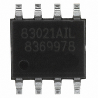
ICS83021AMILF IDT, Integrated Device Technology Inc, ICS83021AMILF Datasheet - Page 5

ICS83021AMILF
Manufacturer Part Number
ICS83021AMILF
Description
IC FANOUT BUFFER SGL I/O 8-SOIC
Manufacturer
IDT, Integrated Device Technology Inc
Series
HiPerClockS™r
Type
Buffer/Driver, Translatorr
Datasheet
1.ICS83021AMILF.pdf
(12 pages)
Specifications of ICS83021AMILF
Number Of Circuits
1
Ratio - Input:output
1:1
Differential - Input:output
Yes/No
Input
HCSL, LVDS, LVHSTL, LVPECL, SSTL
Output
LVCMOS, LVTTL
Frequency - Max
350MHz
Voltage - Supply
2.375 V ~ 3.6 V
Operating Temperature
-40°C ~ 85°C
Mounting Type
Surface Mount
Package / Case
8-SOIC
Frequency-max
350MHz
Logical Function
Translator
Operating Supply Voltage (typ)
2.5/3.3V
Package Type
SOIC
Operating Supply Voltage (max)
3.6V
Operating Supply Voltage (min)
2.375V
Abs. Propagation Delay Time
2.5ns
Mounting
Surface Mount
Pin Count
8
Operating Temperature (min)
-40C
Operating Temperature (max)
85C
Operating Temperature Classification
Industrial
Lead Free Status / RoHS Status
Lead free / RoHS Compliant
Other names
800-1100
800-1100-5
800-1100
83021AMILF
800-1100-5
800-1100
83021AMILF
Available stocks
Company
Part Number
Manufacturer
Quantity
Price
Company:
Part Number:
ICS83021AMILF
Manufacturer:
ICS
Quantity:
5
Additive Phase Jitter
The spectral purity in a band at a specific offset from the
fundamental compared to the power of the fundamental is called
the dBc Phase Noise. This value is normally expressed using a
Phase noise plot and is most often the specified plot in many
applications. Phase noise is defined as the ratio of the noise power
present in a 1Hz band at a specified offset from the fundamental
frequency to the power value of the fundamental. This ratio is
expressed in decibels (dBm) or a ratio of the power in the 1Hz band
As with most timing specifications, phase noise measurements
has issues relating to the limitations of the equipment. Often the
noise floor of the equipment is higher than the noise floor of the
IDT™ / ICS™ LVCMOS/LVTTL TRANSLATOR
ICS83021I
1-TO-1 DIFFERENTIAL-TO-LVCMOS/LVTTL TRANSLATOR
Offset Frequency (Hz)
5
to the power in the fundamental. When the required offset is
specified, the phase noise is called a dBc value, which simply
means dBm at a specified offset from the fundamental. By
investigating jitter in the frequency domain, we get a better
understanding of its effects on the desired application over the
entire time record of the signal. It is mathematically possible to
calculate an expected bit error rate given a phase noise plot.
device. This is illustrated above. The device meets the noise floor
of what is shown, but can actually be lower. The phase noise is
dependent on the input source and measurement equipment.
12kHz to 20MHz = 0.21ps (typical)
Additive Phase Jitter @ 100MHz
ICS83031AMI REV. C OCTOBER 31, 2008


