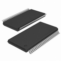
IDT5T9070PAGI IDT, Integrated Device Technology Inc, IDT5T9070PAGI Datasheet - Page 4

IDT5T9070PAGI
Manufacturer Part Number
IDT5T9070PAGI
Description
IC CLK BUFFER/DVR 1:10 48TSSOP
Manufacturer
IDT, Integrated Device Technology Inc
Series
TeraBuffer™ JRr
Type
Fanout Buffer (Distribution)r
Datasheet
1.IDT5T9070PAGI.pdf
(7 pages)
Specifications of IDT5T9070PAGI
Number Of Circuits
1
Ratio - Input:output
1:10
Differential - Input:output
No/No
Input
LVTTL
Output
LVTTL
Frequency - Max
200MHz
Voltage - Supply
2.3 V ~ 2.7 V
Operating Temperature
-40°C ~ 85°C
Mounting Type
Surface Mount
Package / Case
48-TSSOP
Frequency-max
200MHz
Number Of Outputs
10
Operating Supply Voltage (max)
2.7V
Operating Temp Range
-40C to 85C
Propagation Delay Time
3.5ns
Operating Supply Voltage (min)
2.3V
Mounting
Surface Mount
Pin Count
48
Operating Supply Voltage (typ)
2.5V
Package Type
TSSOP
Quiescent Current
2mA
Input Frequency
200MHz
Operating Temperature Classification
Industrial
Lead Free Status / RoHS Status
Lead free / RoHS Compliant
Other names
5T9070PAGI
800-1984-5
IDT5T9070PAGI
800-1984-5
IDT5T9070PAGI
Available stocks
Company
Part Number
Manufacturer
Quantity
Price
Company:
Part Number:
IDT5T9070PAGI
Manufacturer:
ADI
Quantity:
184
Part Number:
IDT5T9070PAGI
Manufacturer:
IDT
Quantity:
20 000
POWER SUPPLY CHARACTERISTICS
NOTE:
1. The termination resistors are excluded from these measurements.
AC ELECTRICAL CHARACTERISTICS OVER OPERATING RANGE
Skew Parameters
Propagation Delay
Output Gate Enable/Disable Delay
NOTES:
1. Skew measured between all outputs under identical input and output transitions and load conditions on any one device.
2. Skew measured is the difference between propagation delay times t
3. Skew measured is the magnitude of the difference in propagation times between any outputs of two devices, given identical transitions and load conditions at identical V
4. Guaranteed by design.
INPUT AC TEST CONDITIONS
NOTES:
1. A nominal 1.25V timing measurement reference level is specified to allow constant, repeatable results in an automatic test equipment (ATE) environment.
2. The input signal edge rate of 2V/ns or greater is to be maintained in the 10% to 90% range of the input waveform.
IDT5T9070
2.5V SINGLE DATA RATE 1:10 CLOCK BUFFER TERABUFFER JR.
Symbol
Symbol
and temperature.
Symbol
t
t
t
I
I
SK
t
SK
I
SK
t
t
t
t
V
DDQ
DDD
V
R
PGD
TOT
V
PLH
PHL
PGE
t
f
t
(
O
R
F
TH
, t
(
(
IH
IL
PP
O
P
F
)
)
)
Quiescent V
Dynamic V
Current per Output
Total Power V
Parameter
Input HIGH Voltage
Input LOW Voltage
Input Timing Measurement Reference Level
Input Signal Edge Rate
Parameter
DD
Parameter
Same Device Output Pin-to-Pin Skew
Pulse Skew
Part-to-Part Skew
Propagation Delay A to Qn
Output Rise Time (20% to 80%)
Output Fall Time (20% to 80%)
Frequency Range
Output Gate Enable to Qn
Output Gate Enable to Qn Driven to GL Designated Level
DD
DD
Power Supply
Power Supply Current
Supply Current
(2)
(2)
(3)
V
Outputs enabled, All outputs unloaded
V
V
V
DD
DD
DD
DD
(1)
(1)
PHL
= Max., Reference Clock = LOW
= 2.5V., F
= 2.5V., F
= Max., V
and t
Test Conditions
PLH
REFERENCE CLOCK
REFERENCE CLOCK
DD
of any output under identical input and output transitions and load conditions on any one device.
= Max., C
4
(1)
L
= 0pF
= 100MHz, C
= 200MHz, C
L
L
= 15pF
= 15pF
Min.
350
350
—
—
—
—
—
—
—
INDUSTRIAL TEMPERATURE RANGE
Typ.
Typ.
150
100
1.5
70
—
—
—
—
—
—
—
—
—
Value
V
V
DD
0
2
DD
(4)
/2
Max
Max
200
150
300
300
850
850
200
3.5
90
25
2
2
3
Units
V/ns
V
V
V
μA/MHz
MHz
Unit
Unit
mA
mA
DD
ps
ps
ps
ns
ps
ps
ns
ns
levels


