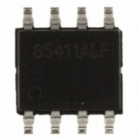
ICS85411AMLF IDT, Integrated Device Technology Inc, ICS85411AMLF Datasheet - Page 11

ICS85411AMLF
Manufacturer Part Number
ICS85411AMLF
Description
IC FANOUT BUFF DIFF-LVDS 8-SOIC
Manufacturer
IDT, Integrated Device Technology Inc
Series
HiPerClockS™r
Type
Fanout Buffer (Distribution)r
Datasheet
1.ICS85411AMLF.pdf
(15 pages)
Specifications of ICS85411AMLF
Number Of Circuits
1
Ratio - Input:output
1:2
Differential - Input:output
Yes/Yes
Input
HCSL, LVDS, LVHSTL, LVPECL, SSTL
Output
LVDS
Frequency - Max
650MHz
Voltage - Supply
2.97 V ~ 3.63 V
Operating Temperature
0°C ~ 70°C
Mounting Type
Surface Mount
Package / Case
8-SOIC
Frequency-max
650MHz
Number Of Outputs
4
Operating Supply Voltage (max)
3.63V
Operating Temp Range
0C to 70C
Propagation Delay Time
2.5ns
Operating Supply Voltage (min)
2.97V
Mounting
Surface Mount
Pin Count
8
Operating Supply Voltage (typ)
3.3V
Package Type
SOIC
Duty Cycle
53%
Operating Temperature Classification
Commercial
Lead Free Status / RoHS Status
Lead free / RoHS Compliant
Other names
800-1184
800-1184-5
800-1184
85411AMLF
800-1184-5
800-1184
85411AMLF
Available stocks
Company
Part Number
Manufacturer
Quantity
Price
Company:
Part Number:
ICS85411AMLF
Manufacturer:
IDT
Quantity:
2 500
Part Number:
ICS85411AMLF
Manufacturer:
IDT
Quantity:
20 000
Company:
Part Number:
ICS85411AMLFT
Manufacturer:
TOSHIBA
Quantity:
272 000
T
IDT
This section provides information on power dissipation and junction temperature for the ICS85411.
Equations and example calculations are also provided.
1. Power Dissipation.
The total power dissipation for the ICS85411 is the sum of the core power plus the power dissipated in the load(s).
The following is the power dissipation for V
2. Junction Temperature.
Junction temperature, Tj, is the temperature at the junction of the bond wire and bond pad and directly affects the reliability of the
device. The maximum recommended junction temperature for HiPerClockS
In order to calculate junction temperature, the appropriate junction-to-ambient thermal resistance
moderate air flow of 200 linear feet per minute and a multi-layer board, the appropriate value is 103.3°C/W per Table 5 below.
Therefore, Tj for an ambient temperature of 70°C with all outputs switching is:
This calculation is only an example. Tj will obviously vary depending on the number of loaded outputs, supply voltage, air flow, and
the type of board (multi-layer).
ABLE
ICS85411
LOW SKEW, 1-TO-2 DIFFERENTIAL-TO-LVDS FANOUT BUFFER
™
The equation for Tj is as follows: Tj =
Tj = Junction Temperature
Pd_total = Total Device Power Dissipation (example calculation is in section 1 above)
T
70°C + 0.182W * 103.3°C/W = 88.8°C. This is below the limit of 125°C.
/ ICS
JA
A
5. T
= Ambient Temperature
= Junction-to-Ambient Thermal Resistance
Single-Layer PCB, JEDEC Standard Test Boards
Multi-Layer PCB, JEDEC Standard Test Boards
NOTE: Most modern PCB designs use multi-layered boards. The data in the second row pertains to most designs.
Power (core)
™
DIFFERENTIAL-TO-LVDS FANOUT BUFFER
HERMAL
R
ESISTANCE
MAX
= V
DD_MAX
* I
JA
DD_MAX
FOR
8-L
= 3.63V * 50mA = 181.5mW
JA
DD
JA
EAD
= 3.3V + 10% = 3.63V, which gives worst case results.
P
by Velocity (Linear Feet per Minute)
* Pd_total + T
OWER
SOIC, F
ORCED
C
A
ONSIDERATIONS
C
153.3°C/W
112.7°C/W
11
ONVECTION
0
TM
devices is 125°C.
128.5°C/W
103.3°C/W
200
ICS85411AM REV. C JANUARY 20, 2009
JA
115.5°C/W
must be used. Assuming a
97.1°C/W
500


