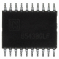
ICS8543BGLF IDT, Integrated Device Technology Inc, ICS8543BGLF Datasheet - Page 10

ICS8543BGLF
Manufacturer Part Number
ICS8543BGLF
Description
IC FANOUT BUFF DIFF-LVDS 20TSSOP
Manufacturer
IDT, Integrated Device Technology Inc
Type
Fanout Buffer (Distribution), Multiplexerr
Series
HiPerClockS™r
Datasheet
1.ICS8543BGLF.pdf
(18 pages)
Specifications of ICS8543BGLF
Number Of Circuits
1
Ratio - Input:output
2:4
Differential - Input:output
Yes/Yes
Input
CML, HCSL, LVDS, LVHSTL, LVPECL, SSTL
Output
LVDS
Frequency - Max
800MHz
Voltage - Supply
3.135 V ~ 3.465 V
Operating Temperature
0°C ~ 70°C
Mounting Type
Surface Mount
Package / Case
20-TSSOP
Frequency-max
800MHz
Number Of Clock Inputs
2
Mode Of Operation
Differential
Output Frequency
800MHz
Output Logic Level
LVDS
Operating Supply Voltage (min)
3.135V
Operating Supply Voltage (typ)
3.3V
Operating Supply Voltage (max)
3.465V
Package Type
TSSOP
Operating Temp Range
0C to 70C
Operating Temperature Classification
Commercial
Mounting
Surface Mount
Pin Count
20
Lead Free Status / RoHS Status
Lead free / RoHS Compliant
Other names
800-1186
800-1186-5
800-1186
8543BGLF
800-1186-5
800-1186
8543BGLF
Available stocks
Company
Part Number
Manufacturer
Quantity
Price
Company:
Part Number:
ICS8543BGLF
Manufacturer:
IDT
Quantity:
755
Part Number:
ICS8543BGLFT
Manufacturer:
IDT
Quantity:
20 000
ICS8543 Data Sheet
Parameter Measurement Information, continued
Output Short Circuit Current Setup
Applications Information
Wiring the Differential Input to Accept Single-Ended Levels
Figure 2 shows how a differential input can be wired to accept single
ended levels. The reference voltage V
the bias resistors R1 and R2. The bypass capacitor (C1) is used to
help filter noise on the DC bias. This bias circuit should be located as
close to the input pin as possible. The ratio of R1 and R2 might need
to be adjusted to position the V
swing. For example, if the input clock swing is 2.5V and V
R1 and R2 value should be adjusted to set V
below are for when both the single ended swing and V
same voltage. This configuration requires that the sum of the output
impedance of the driver (Ro) and the series resistance (Rs) equals
the transmission line impedance. In addition, matched termination at
the input will attenuate the signal in half. This can be done in one of
two ways. First, R3 and R4 in parallel should equal the transmission
Figure 1. Recommended Schematic for Wiring a Differential Input to Accept Single-ended Levels
ICS8543BG REVISION E DECEMBER 17, 2010
DC Input
V
DD
LVDS
REF
in the center of the input voltage
REF
= V
REF
CC
at 1.25V. The values
/2 is generated by
out
out
DD
I
OSB
I
OS
DD
are at the
= 3.3V,
10
Power Off Leakage Setup
line impedance. For most 50Ω applications, R3 and R4 can be 100Ω.
The values of the resistors can be increased to reduce the loading for
slower and weaker LVCMOS driver. When using single-ended
signaling, the noise rejection benefits of differential signaling are
reduced. Even though the differential input can handle full rail
LVCMOS signaling, it is recommended that the amplitude be
reduced. The datasheet specifies a lower differential amplitude,
however this only applies to differential signals. For single-ended
applications, the swing can be larger, however V
than -0.3V and V
of the recommended components might not be used, the pads
should be placed in the layout. They can be utilized for debugging
purposes. The datasheet specifications are characterized and
guaranteed by using a differential signal.
IH
LOW SKEW, 1-to-4, DIFFERENTIAL-TO-LVDS FANOUT BUFFER
cannot be more than V
LVDS
©2010 Integrated Device Technology, Inc.
DD
+ 0.3V. Though some
IL
I
cannot be less
OFF
V
DD


