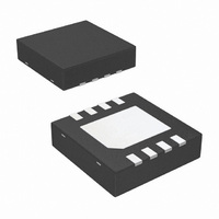
LMV112SD/NOPB National Semiconductor, LMV112SD/NOPB Datasheet - Page 12

LMV112SD/NOPB
Manufacturer Part Number
LMV112SD/NOPB
Description
IC CLOCK BUFFER DUAL 40MHZ 8-LLP
Manufacturer
National Semiconductor
Type
Fanout Buffer (Distribution)r
Datasheet
1.LMV112SDNOPB.pdf
(14 pages)
Specifications of LMV112SD/NOPB
Number Of Circuits
2
Ratio - Input:output
2:2
Differential - Input:output
No/No
Input
Clock
Output
Clock
Frequency - Max
40MHz
Voltage - Supply
2.4 V ~ 5.0 V
Operating Temperature
-40°C ~ 85°C
Mounting Type
Surface Mount
Package / Case
8-LLP
Frequency-max
40MHz
Slew Rate
110V/µs
Supply Voltage Range
2.4V To 5V
Logic Case Style
LLP
No. Of Pins
8
Operating Temperature Range
-40°C To +85°C
Msl
MSL 1 - Unlimited
Single Supply Voltage Min (+v)
2.4V
Rohs Compliant
Yes
Amplifier Case Style
LLP
For Use With
LMV112SDEVAL - BOARD EVALUATION FOR LMV112SD
Lead Free Status / RoHS Status
Lead free / RoHS Compliant
Other names
*LMV112SD
LMV112SD
LMV112SDNOPB
LMV112SDNOPBTR
LMV112SDNOPBTR
LMV112SDTR
LMV112SD
LMV112SDNOPB
LMV112SDNOPBTR
LMV112SDNOPBTR
LMV112SDTR
Available stocks
Company
Part Number
Manufacturer
Quantity
Price
Company:
Part Number:
LMV112SD/NOPB
Manufacturer:
TI
Quantity:
144
www.national.com
Application Section
GENERAL
The LMV112 is designed to minimize the effects of spurious
signals from the base band chip to the oscillator. Also the
influence of varying load resistance and capacitance to the
oscillator is minimized, while the drive capability is in-
creased.
The inputs of the LMV112 are internally biased at 1V, making
AC coupling possible without external bias resistors.
To optimize current consumption, the buffer not in use can
be disabled by connecting the enable pin to V
The LMV112 has no internal ground reference; therefore,
either single or split supply configurations can be used.
The LMV112 is an easy replacement for discrete circuitry. It
simplifies board layout and minimizes the effect of layout
related parasitic components.
INPUT CONFIGURATION
AC coupling is made possible by biasing the input. A large
DC load at the oscillator input could change the load imped-
ance and therefore it’s oscillating frequency. To avoid exter-
nal resistors the inputs are internally biased. This biasing is
set at 1V as depicted in Figure 1. Because this biasing is set
at 1V, the maximum amplitude of the AC signal is 2 V
The coupling capacitance should be large enough to let the
AC signal pass. This is a unity gain buffer with rail-to-rail
inputs and outputs.
FREQUENCY PULLING
Frequency pulling is the frequency variation of an oscillator
caused by a varying load. In the typical application, the load
of the oscillator is a fixed capacitor (C1) and the input
impedance of the buffer.
To keep the input impedance as constant as possible, the
input is biased at 1V, even when the part is disabled. A
simplified schematic of the input configuration is shown in
Figure 1.
ISOLATION AND CROSSTALK
Output to input isolation prevents the clock from being af-
fected by spurious signals generated by the digital blocks at
the output buffer. See the characteristic graphic entitled “Iso-
lation Output to Input vs. Frequency.”
FIGURE 1. Input Configuration
SS
.
20135344
PP
.
12
A block diagram of the isolation is shown in Figure 2.
Crosstalk rejection between buffers prevents signals from
affecting each other. Figure 2 shows a Base band IC and a
Bluetooth module as examples of this. See the characteristic
graphic labeled “Crosstalk Rejection vs. Frequency” for more
information.
DRIVING CAPACITIVE LOADS
Each buffer can drive a capacitive load. Be aware that every
capacitor directly connected to the output becomes part of
the loop of the buffer. In most applications the load consists
of the capacitance of copper tracks and the input capaci-
tance of the application blocks. Capacitance reduces the
gain/phase margin and increases the instability. It leads to
peaking in the frequency response and in extreme situations
oscillations can occur. To drive a large capacitive load it is
recommended that a series resistor is included between the
buffer and the load capacitor. The best value for this isolation
resistance is often found by experimentation.
The LMV112 datasheet reflects measurements with capaci-
tance loads of 20 pF at the output of the buffers. Most
common applications will probably use a lower capacitance
load, which will result in lower peaking and significantly
greater bandwidth, see Figure 3.
FIGURE 2. Isolation Block Diagram
FIGURE 3. Bandwidth and Peaking
20135346
20135345


