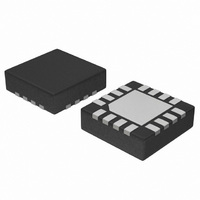
NB6N11SMNG ON Semiconductor, NB6N11SMNG Datasheet - Page 9

NB6N11SMNG
Manufacturer Part Number
NB6N11SMNG
Description
IC BUFFER/XLATOR LVDS 16-QFN
Manufacturer
ON Semiconductor
Series
AnyLevel™ ECLinPS MAX™r
Type
Fanout Buffer (Distribution), Translatorr
Specifications of NB6N11SMNG
Number Of Circuits
1
Ratio - Input:output
1:2
Differential - Input:output
Yes/Yes
Input
CML, LVCMOS, LVDS, LVPECL, LVTTL
Output
LVDS
Frequency - Max
2GHz
Voltage - Supply
3 V ~ 3.6 V
Operating Temperature
-40°C ~ 85°C
Mounting Type
Surface Mount
Package / Case
16-TFQFN Exposed Pad
Frequency-max
2GHz
Number Of Outputs
4
Max Input Freq
>2000 MHz
Propagation Delay (max)
0.47 ns @ 3V to 3.6V
Supply Voltage (max)
3.6 V
Supply Voltage (min)
3 V
Maximum Operating Temperature
+ 85 C
Minimum Operating Temperature
- 40 C
Mounting Style
SMD/SMT
Lead Free Status / RoHS Status
Lead free / RoHS Compliant
Other names
NB6N11SMNG
NB6N11SMNGOS
NB6N11SMNGOS
Available stocks
Company
Part Number
Manufacturer
Quantity
Price
Company:
Part Number:
NB6N11SMNG
Manufacturer:
ON
Quantity:
311
Company:
Part Number:
NB6N11SMNG
Manufacturer:
ON Semiconductor
Quantity:
4
Part Number:
NB6N11SMNG
Manufacturer:
ON/安森美
Quantity:
20 000
†For information on tape and reel specifications, including part orientation and tape sizes, please refer to our Tape and Reel Packaging
ORDERING INFORMATION
Specifications Brochure, BRD8011/D.
NB6N11SMNG
NB6N11SMNR2G
V
V
th
V
thmax
GND
thmin
Figure 20. Differential Input Driven Single−Ended
V
V
V
IH
IL
CC
V
th
Device
D
Figure 22. V
D
Figure 18. Typical LVDS Termination for Output Driver and Device Evaluation
V
th
th
LVDS
Driver
Device
Diagram
D
D
Q
Q
N
N
V
V
V
V
QFN−16, 3 X 3 mm
QFN−16, 3 X 3 mm
IHmax
ILmax
IHmin
ILmin
(Pb−Free)
(Pb−Free)
Figure 17. AC Reference Measurement
Package
Q
Q
Q
Q
D
D
t
PLH
Figure 19. LVDS Output
http://onsemi.com
Z
Z
o
o
= 50 W
= 50 W
9
100 W
V
OS
Figure 21. Differential Inputs Driven Differentially
GND
V
V
V
t
INPP
OUTPP
PHL
CC
V
CMR
V
= V
D
D
OD
= V
IH
3000 / Tape & Reel
(D) − V
OH
Figure 23. V
123 Units / Rail
V
V
OH
OL
Shipping
LVDS
Receiver
Device
(Q) − V
IL
D
D
(D)
OL
†
(Q)
CMR
Diagram
V
V
V
V
V
V
V
INPP
IH(MAX)
IL
IH
IL
IH
IL(MIN)
= V
IHD
− V
ILD


