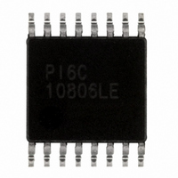
PI6C10806LE Pericom Semiconductor, PI6C10806LE Datasheet - Page 2

PI6C10806LE
Manufacturer Part Number
PI6C10806LE
Description
IC CLOCK BUFF 250MHZ 16TSSOP
Manufacturer
Pericom Semiconductor
Type
Fanout Buffer (Distribution)r
Datasheet
1.PI6C10806LE.pdf
(7 pages)
Specifications of PI6C10806LE
Number Of Circuits
1
Ratio - Input:output
1:6
Differential - Input:output
No/No
Input
LVCMOS, Crystal
Output
Crystal, LVCMOS
Frequency - Max
250MHz
Voltage - Supply
1.6 V ~ 2 V, 2.375 V ~ 2.625 V
Operating Temperature
-40°C ~ 85°C
Mounting Type
Surface Mount
Package / Case
16-TSSOP
Frequency-max
250MHz
Lead Free Status / RoHS Status
Lead free / RoHS Compliant
2.5V Absolute Maximum Ratings
2.5V I/O DC Characteristics
Notes:
2.5V I/O AC Characteristics
Notes:
3.
4. These parameters are guaranteed, but not tested.
1. For Max. or Min. conditions, use appropriate operating range values.
2. Typical values are at V
1. Unless noted otherwise, all parameters are tested with xtal @ f <= Fxtal_max,; outputs are terminated @ 50Ω to
2. External clock source is driving XTAL_IN input
Parameters
f
t
t
t
t
Storage Temperature ...........................................................–65°C to +150°C
V
Output Voltage (max. 3.6V) .......................................... –0.5V to V
Input Voltage (max 3.6V) .............................................. –0.5V to V
DC
R
SK(O)
DIS,
OUT
/t
DD,
Parameters
V
F
Identical conditions: loading, transitions, supply voltage, temperature, package type and speed grade.
Min & Max delay is 4 cycles.
V
V
V
V
t
DDO
EN
OH
OL
IH
(3)
V
IL
07-0201
( 4)
DDO
Voltage ...............................................................–0.5V to +3.6V
I/O Supply Voltage
Input HIGH Voltage
Input LOW Voltage
Output High Voltage
Output LOW Voltage
Output Frequency
Output Duty Cycle
CLKn Rise/Fall Time
Output to Output Skew between any two
outputs of the same device @ same transition
Output Enable/Disable
Description
CC
= 2.5V, +25°C ambient and maximum loading.
(Over Operating Range: V
De scrip tion
(Over Operating Range: V
Logic HIGH level
Logic LOW level
V
V
DDO
DDO
(Above which the useful life may be impaired. For user guidelines only, not tested.)
= Min., V
= Min., V
Test Conditions
IN
1.8V/2.5V Low Skew 1:6 Crystal to LVCMOS Clock Buffer
IN
= V
= V
DD
DD
IH
IH
/V
2
or V
= 2.5V ± 5%, T
or V
DD
DD
DDO
Test Conditions
External Clock
+0.5V
+0.5V
IL
IL
Using Crystal
20% to 80%
(1)
= 2.5V ± 5%, T
@ V
@V
@V
I
I
I
I
OH
OH
OL
OL
DDO
DDO
DDO
= 1mA
= 8mA
= -1mA
= -8mA
Note:
Stresses greater than those listed under MAXIMUM
RAT INGS may cause permanent damage to the
device. This is a stress rating only and functional op er a tion
of the device at these or any other con di tions above those
indicated in the operational sec tions of this spec i fi ca tion is
not implied. Ex po sure to absolute maximum rating con di -
tions for extended periods may affect re li abil i ty.
/2
/2
A
/2
= -40° to 85°C)
(2)
(1)
A
= -40° to 85°C)
2.375
Min.
Min.
150
-0.3
1.7
10
47
0
2
2
Typ.
Typ
V
2.5
`
DDO
(2)
/2
, see waveforms.
V
Max.
250
800
Max.
2.625
DD
40
53
60
PS8823C
4
0.7
0.4
0.4
PI6C10806
+0.3
cycles
Units
MHz
Units
%
ps
ps
09/12/07
V
V


