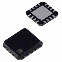
ADCLK925BCPZ-R2 Analog Devices Inc, ADCLK925BCPZ-R2 Datasheet - Page 6

ADCLK925BCPZ-R2
Manufacturer Part Number
ADCLK925BCPZ-R2
Description
IC CLOCK/DATA BUFFER 1:2 16LFCSP
Manufacturer
Analog Devices Inc
Series
SIGer
Type
Fanout Buffer (Distribution), Datar
Datasheet
1.ADCLK905BCPZ-R7.pdf
(16 pages)
Specifications of ADCLK925BCPZ-R2
Number Of Circuits
1
Ratio - Input:output
1:2
Differential - Input:output
Yes/Yes
Input
Clock
Output
ECL, NECL, PECL
Frequency - Max
7.5GHz
Voltage - Supply
2.375 V ~ 3.63 V
Operating Temperature
-40°C ~ 125°C
Mounting Type
Surface Mount
Package / Case
16-LFCSP
Frequency-max
7.5GHz
Clock Ic Type
Clock Buffer
Frequency
7.5GHz
No. Of Outputs
2
Supply Current
77mA
Supply Voltage Range
2.375V To 3.63V
Digital Ic Case Style
LFCSP
No. Of Pins
16
Lead Free Status / RoHS Status
Lead free / RoHS Compliant
For Use With
ADCLK925/PCBZ - BOARD EVAL FOR ADCLK925 16LFCSP
Lead Free Status / RoHS Status
Lead free / RoHS Compliant, Lead free / RoHS Compliant
ADCLK905/ADCLK907/ADCLK925
PIN CONFIGURATIONS AND FUNCTION DESCRIPTIONS
Table 4. Pin Function Descriptions for 1:1 ADCLK905 Buffer
Pin No.
1
2
3, 4, 5, 6,
9, 10
7, 14
8, 13
11
12
15
16
Heat Sink
Table 5. Pin Function Descriptions for Dual 1:1 ADCLK907 Buffer
Pin No.
1
2
3
4
5
6
7, 14
8, 13
9
Mnemonic
D
D
NC
V
V
Q
Q
V
V
NC
Mnemonic
D1
D1
D2
D2
V
V
V
V
Q2
EE
CC
REF
T
T
REF
EE
CC
2
2
Description
Noninverting Input.
Inverting Input.
No Connect. No physical connection to the die.
Negative Supply Voltage.
Positive Supply Voltage.
Inverting Output.
Noninverting Output.
Reference Voltage. Reference voltage for biasing ac-coupled inputs.
Center Tap. Center tap of 100 Ω input resistor.
No Connect. The metallic back surface of the package is not electrically connected to any part of the circuit.
It can be left floating for optimal electrical isolation between the package handle and the substrate of the die.
It can also be soldered to the application board if improved thermal and/or mechanical stability is desired.
Exposed metal at the corners of the package is connected to this back surface. Allow sufficient clearance
to vias and other components.
Description
Noninverting Input 1.
Inverting Input 1.
Noninverting Input 2.
Inverting Input 2.
Center Tap 2. Center tap of 100 Ω input resistor, Channel 2.
Reference Voltage 2. Reference voltage for biasing ac-coupled inputs, Channel 2.
Negative Supply Voltage.
Positive Supply Voltage. Pin 8 and Pin 13 are not strapped internally.
Inverting Output 2.
NC = NO CONNECT
Figure 4. ADCLK905 Pin Configuration
Figure 5. ADCLK907 Pin Configuration
D1
D1
D2
D2
1
2
3
4
NC
NC
D
D
Rev. 0 | Page 6 of 16
ADCLK907
(Not to Scale)
1
2
3
4
TOP VIEW
PIN 1
INDICATOR
ADCLK905
(Not to Scale)
TOP VIEW
PIN 1
INDICATOR
12 Q1
11 Q1
10 Q2
9 Q2
12 Q
11 Q
10 NC
9 NC


