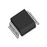
LV810FI IDT, Integrated Device Technology Inc, LV810FI Datasheet - Page 13

LV810FI
Manufacturer Part Number
LV810FI
Description
IC BUFFER/CLOCK DRIVER 20-SSOP
Manufacturer
IDT, Integrated Device Technology Inc
Type
Fanout Buffer (Distribution)r
Datasheet
1.LV810RILFT.pdf
(14 pages)
Specifications of LV810FI
Number Of Circuits
1
Ratio - Input:output
1:10
Differential - Input:output
No/No
Input
Clock
Output
TTL
Frequency - Max
133MHz
Voltage - Supply
1.425 V ~ 2.625 V
Operating Temperature
-40°C ~ 85°C
Mounting Type
Surface Mount
Package / Case
20-SSOP
Frequency-max
133MHz
Number Of Outputs
10
Operating Supply Voltage (max)
2.625V
Operating Temp Range
-40C to 85C
Propagation Delay Time
3.5ns
Operating Supply Voltage (min)
1.425V
Mounting
Surface Mount
Pin Count
20
Operating Supply Voltage (typ)
2.5V
Package Type
SSOP
Input Frequency
133MHz
Duty Cycle
60%
Operating Temperature Classification
Industrial
Lead Free Status / RoHS Status
Contains lead / RoHS non-compliant
Revision History
IDT™ / ICS™ BUFFER/CLOCK DRIVER
Rev.
ICSLV810
BUFFER/CLOCK DRIVER
G
A
B
C
D
E
H
F
K. Beckmeyer
K. Beckmeyer
Originator
P.Griffith
P.Griffith
P.Griffith
P.Griffith
03/25/05 New device/datasheet.
05/02/05 Released from Preliminary to final; changed Short Circuit Current parameter in 2.5 V DC
05/12/05 Added bullet in “Features” for operating voltage of 2.5 V on Bank A and specified that
06/21/05 Added 209 mil 20-pin SSOP package and ordering info.
07/27/05 Specified operating voltage on Bank A from 1.5V to 2.5V; Added figures 4 and 5 on page
10/13/05 Added “LF” packaging and ordering info to both “R” and”F” packages.
12/17/09 Added EOL note for non-gren parts.
05/13/10 Removed EOL note and non-green orderables.
Date
Description of Change
Char table to ±80 mA; changed Short Circuit Current parameter in 1.5 V DC Char table to
±35 mA
operating voltages of 1.5 and 2.5 V are on Banks B and C; changed block diagram input
and pin 1 from IN to CLKIN; removed +1.5 V spec from pin 4 and pin 8 descriptions; added
“VDDA + 1.2 V” to “All Inputs and Outputs” section of Absolute Maximum Ratings; added
min and max values for Banks A, B, and C “Power Supply Voltage” in Recommended
Operating Conditions; expanded DC Electrical Char tables in to include a separate table
for Banks A, B, and C; expanded AC Electrical Char tables in to include a separate table
for Banks A, B, and C;
10 to explain Pulse Skew and Part-to-Part Skew; Changed Output Frequency Max
Specification to 133MHz in AC Electrical Char tables for Banks A, B, and C; Added Duty
Cycle Spec for VDD = 1.5V in AC Electrical Char tables for Banks A, B, C; Changed CLK
conditions in DC Electrical Char tables on Banks B and C; removed SOIC package.
13
ICSLV810
FAN OUT BUFFER
REV H 051310


