MK3805RI IDT, Integrated Device Technology Inc, MK3805RI Datasheet - Page 3
MK3805RI
Manufacturer Part Number
MK3805RI
Description
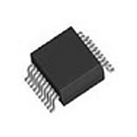
IC BUFFER/CLOCK DRIVER 20-QSOP
Manufacturer
IDT, Integrated Device Technology Inc
Type
Fanout Buffer (Distribution)r
Datasheet
1.MK3805RILFTR.pdf
(7 pages)
Specifications of MK3805RI
Number Of Circuits
2
Ratio - Input:output
1:5
Differential - Input:output
No/No
Input
LVCMOS
Output
LVCMOS
Frequency - Max
100MHz
Voltage - Supply
3.13 V ~ 3.46 V
Operating Temperature
-40°C ~ 85°C
Mounting Type
Surface Mount
Package / Case
20-QSOP
Frequency-max
100MHz
Number Of Outputs
10
Operating Supply Voltage (max)
3.46V
Operating Temp Range
-40C to 85C
Propagation Delay Time
4.5ns
Operating Supply Voltage (min)
3.13V
Mounting
Surface Mount
Pin Count
20
Operating Supply Voltage (typ)
3.3V
Package Type
QSOP
Quiescent Current
30uA
Duty Cycle
55%
Operating Temperature Classification
Industrial
Lead Free Status / RoHS Status
Contains lead / RoHS non-compliant


External Components
The MK3805 requires a minimum number of external
components for proper operation.
Decoupling Capacitors
Decoupling capacitors of 0.01µF must be connected
between VDD and GND, as close to these pins as possible.
For optimum device performance, the decoupling capacitors
should be mounted on the component side of the PCB.
Avoid the use of vias in the decoupling circuit.
Series Termination Resistor
When the PCB trace between the clock outputs and the
loads are over 1 inch, series termination should be used. To
series terminate a 50 trace (a commonly used trace
impedance) place a 33 resistor in series with the clock line,
as close to the clock output pin as possible. The nominal
impedance of the clock output is 20 .
Absolute Maximum Ratings
IDT™ BUFFER/CLOCK DRIVER
MK3805
BUFFER/CLOCK DRIVER
Stresses above the ratings listed below can cause permanent damage to the MK3805. These ratings, which are
standard values for IDT commercially rated parts, are stress ratings only. Functional operation of the device at these
or any other conditions above those indicated in the operational sections of the specifications is not implied.
Exposure to absolute maximum rating conditions for extended periods can affect product reliability. Electrical
parameters are guaranteed only over the recommended operating temperature range.
Supply Voltage, VDD
All Inputs and Outputs
Ambient Operating Temperature
Storage Temperature
Junction Temperature
Soldering Temperature
Item
3
PCB Layout Recommendations
For optimum device performance and lowest output phase
noise, the following guidelines should be observed.
1) The 0.01µF decoupling capacitors should be mounted on
the component side of the board as close to the VDD pins
as possible. No vias should be used between the
decoupling capacitors and VDD pins. The PCB trace to VDD
pin should be kept as short as possible, as should the PCB
trace to the ground via.
2) To minimize EMI, the 33 series termination resistor (if
needed) should be placed close to the clock output.
3) An optimum layout is one with all components on the
same side of the board, minimizing vias through the signal
layers. Other signal traces should be routed away from the
MK3805. This includes signal traces just underneath the
device, or on layers adjacent to the ground plane layer used
by the device.
7 V
-0.5 V to VDD+0.5 V
-40 to +85 C
-65 to +150 C
125 C
260 C
Rating
MK3805
FAN OUT BUFFER
REV E 051310
Related parts for MK3805RI
Image
Part Number
Description
Manufacturer
Datasheet
Request
R

Part Number:
Description:
TRANSLATION DEVICE DPI 80-PQFP
Manufacturer:
IDT, Integrated Device Technology Inc
Datasheet:
Part Number:
Description:
IDT PART
Manufacturer:
IDT, Integrated Device Technology Inc
Datasheet:
Part Number:
Description:
IC LIU T1/E1/J1 OCTAL 256PBGA
Manufacturer:
IDT, Integrated Device Technology Inc
Datasheet:

Part Number:
Description:
IC FREQ TIMING GENERATOR 28TSSOP
Manufacturer:
IDT, Integrated Device Technology Inc
Datasheet:
Part Number:
Description:
IC CLK DVR PLL 1:10 40VFQFPN
Manufacturer:
IDT, Integrated Device Technology Inc
Datasheet:
Part Number:
Description:
IC CLK FANOUT BUFFER 1:18 32LQFP
Manufacturer:
IDT, Integrated Device Technology Inc
Datasheet:
Part Number:
Description:
IC CLK FANOUT BUFFER 1:18 32LQFP
Manufacturer:
IDT, Integrated Device Technology Inc
Datasheet:
Part Number:
Description:
IC CK505 VREG/RES 56TSSOP
Manufacturer:
IDT, Integrated Device Technology Inc
Datasheet:

Part Number:
Description:
IC SDRAM CLK DVR 1:10 48-TSSOP
Manufacturer:
IDT, Integrated Device Technology Inc
Datasheet:

Part Number:
Description:
IC CLK DVR PLL 1:10 48TSSOP
Manufacturer:
IDT, Integrated Device Technology Inc
Datasheet:
Part Number:
Description:
IC FLEXPC CLK PROGR P4 56-TSSOP
Manufacturer:
IDT, Integrated Device Technology Inc
Datasheet:
Part Number:
Description:
IC FLEXPC CLK PROGR P4 56-TSSOP
Manufacturer:
IDT, Integrated Device Technology Inc
Datasheet:
Part Number:
Description:
IC FLEXPC CLK PROGR P4 56-SSOP
Manufacturer:
IDT, Integrated Device Technology Inc
Datasheet:

Part Number:
Description:
IC PLL CLK DRIVER 2.5V 28-TSSOP
Manufacturer:
IDT, Integrated Device Technology Inc
Datasheet:
Part Number:
Description:
IC CLOCK DRIVER 2.5V 24-TSSOP
Manufacturer:
IDT, Integrated Device Technology Inc
Datasheet: