IDT49FCT3805EQI IDT, Integrated Device Technology Inc, IDT49FCT3805EQI Datasheet - Page 2
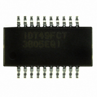
IDT49FCT3805EQI
Manufacturer Part Number
IDT49FCT3805EQI
Description
IC CLK DRIVER DUAL 1-5 20-SSOP
Manufacturer
IDT, Integrated Device Technology Inc
Series
49FCTr
Type
Fanout Buffer (Distribution)r
Datasheet
1.IDT49FCT3805EPYGI.pdf
(7 pages)
Specifications of IDT49FCT3805EQI
Number Of Circuits
2
Ratio - Input:output
1:5
Differential - Input:output
No/No
Input
LVTTL
Output
LVTTL
Frequency - Max
166MHz
Voltage - Supply
3 V ~ 3.6 V
Operating Temperature
-40°C ~ 85°C
Mounting Type
Surface Mount
Package / Case
20-SSOP
Frequency-max
166MHz
Lead Free Status / RoHS Status
Contains lead / RoHS non-compliant
Other names
49FCT3805EQI


ABSOLUTE MAXIMUM RATINGS
NOTE:
1. Stresses greater than those listed under ABSOLUTE MAXIMUM RATINGS may cause
CAPACITANCE (T
NOTE:
1. This parameter is measured at characterization but not tested.
DC ELECTRICAL CHARACTERISTICS OVER OPERATING RANGE
Following Conditions Apply Unless Otherwise Specified
Industrial: T
NOTES:
1. For conditions shown as Max. or Min., use appropriate value specified under Electrical Characteristics for the applicable device type.
2. Typical values are at V
3. Not more than one output should be shorted at one time. Duration of the test should not exceed one second.
4. This parameter is guaranteed but not tested.
5. V
IDT49FCT3805D/E
3.3V CMOS DUAL 1-TO-5 CLOCK DRIVER
Symbol
Symbol
Symbol
C
I
I
permanent damage to the device. This is a stress rating only and functional operation
of the device at these or any other conditions above those indicated in the operational
sections of this specification is not implied. Exposure to absolute maximum rating
conditions for extended periods may affect reliability.
I
I
V
V
T
C
V
OZH
V
ODH
I
V
V
OZL
ODL
OUT
I
I
V
OS
V
T
STG
IH
IL
OH
OL
OH
IN
IH
IK
CC
IL
O
J
I
= Vcc -0.6V at rated current.
A
= -40°C to +85°C, V
Description
Input Power Supply Voltage
Input Voltage
Output Voltage
Junction Temperature
Storage Temperature
Parameter
Input Capacitance
Output Capacitance
Parameter
Input HIGH Level
Input LOW Level
Input HIGH Current
Input LOW Current
High Impedance Output Current
(3-State Outputs Pins)
Clamp Diode Voltage
Output HIGH Current
Output LOW Current
Short Circuit Current
Output HIGH Voltage
Output LOW Voltage
CC
(1)
= 3.3V, 25°C ambient.
A
CC
= +25
Conditions
V
= 3.3V ± 0.3V
V
OUT
IN
= 0V
= 0V
O
C, f = 1.0MHz)
Typ.
—
–0.5 to V
3
–0.5 to +4.6
–0.5 to +5.5
–65 to +165
Max
150
V
V
V
V
V
V
V
V
V
V
V
CC
CC
CC
CC
CC
CC
CC
CC
IN
CC
IN
CC
Max.
= V
= V
(1)
4
6
= Min., I
= 3.3V, V
= 3.3V, V
= Min.
= Min.
+0.5
= Max.
= Max.
= Max.
= Max., V
IH
IH
or V
or V
Unit
pF
pF
Unit
IN
°C
°C
IL
IL
V
V
V
IN
IN
O
= –18mA
Test Conditions
= V
= V
= GND
2
IH
IH
or V
or V
PIN DESCRIPTION
FUNCTION TABLE
NOTE:
1. H = HIGH
(3,4)
L = LOW
Z = High-Impedance
IL
IL
OE
Pin Names
, V
, V
OAn, OBn
OE
IN
A
MON
, OE
H
H
V
V
V
V
O
O
I
I
I
I
I
I
A
L
L
A
OH
OH
OH
OL
OL
OL
, OE
, IN
I
I
O
O
(1)
= 1.5V
= 1.5V
= 5.5V
= GND
= V
= GND
= 12mA
= 8mA
= 100µA
= –12mA
= –8mA
= –100µA
B
B
B
CC
Inputs
(3,4)
(3,4)
3-State Output Enable Inputs (Active LOW)
Clock Inputs
Clock Outputs
Monitor Output
IN
A
H
H
, IN
L
L
B
INDUSTRIAL TEMPERATURE RANGE
V
Min.
–0.5
CC
2.4
2.4
–45
–60
2
—
—
—
—
—
50
—
—
—
- 0.2
(1)
(5)
(5)
Description
OAn, OBn
Typ.
–135
–0.7
–74
0.3
0.2
—
—
—
—
—
—
90
—
—
3
3
H
L
Z
Z
(2)
Outputs
Max.
–180
–240
–1.2
200
5.5
0.8
±1
±1
±1
±1
0.4
0.4
0.2
—
—
—
MON
H
H
Unit
L
L
mA
mA
mA
µA
V
V
V
V
V
Related parts for IDT49FCT3805EQI
Image
Part Number
Description
Manufacturer
Datasheet
Request
R

Part Number:
Description:
TRANSLATION DEVICE DPI 80-PQFP
Manufacturer:
IDT, Integrated Device Technology Inc
Datasheet:
Part Number:
Description:
IDT PART
Manufacturer:
IDT, Integrated Device Technology Inc
Datasheet:
Part Number:
Description:
IC LIU T1/E1/J1 OCTAL 256PBGA
Manufacturer:
IDT, Integrated Device Technology Inc
Datasheet:

Part Number:
Description:
IC FREQ TIMING GENERATOR 28TSSOP
Manufacturer:
IDT, Integrated Device Technology Inc
Datasheet:
Part Number:
Description:
IC CLK DVR PLL 1:10 40VFQFPN
Manufacturer:
IDT, Integrated Device Technology Inc
Datasheet:
Part Number:
Description:
IC CLK FANOUT BUFFER 1:18 32LQFP
Manufacturer:
IDT, Integrated Device Technology Inc
Datasheet:
Part Number:
Description:
IC CLK FANOUT BUFFER 1:18 32LQFP
Manufacturer:
IDT, Integrated Device Technology Inc
Datasheet:
Part Number:
Description:
IC CK505 VREG/RES 56TSSOP
Manufacturer:
IDT, Integrated Device Technology Inc
Datasheet:

Part Number:
Description:
IC SDRAM CLK DVR 1:10 48-TSSOP
Manufacturer:
IDT, Integrated Device Technology Inc
Datasheet:

Part Number:
Description:
IC CLK DVR PLL 1:10 48TSSOP
Manufacturer:
IDT, Integrated Device Technology Inc
Datasheet:
Part Number:
Description:
IC FLEXPC CLK PROGR P4 56-TSSOP
Manufacturer:
IDT, Integrated Device Technology Inc
Datasheet:
Part Number:
Description:
IC FLEXPC CLK PROGR P4 56-TSSOP
Manufacturer:
IDT, Integrated Device Technology Inc
Datasheet:
Part Number:
Description:
IC FLEXPC CLK PROGR P4 56-SSOP
Manufacturer:
IDT, Integrated Device Technology Inc
Datasheet:

Part Number:
Description:
IC PLL CLK DRIVER 2.5V 28-TSSOP
Manufacturer:
IDT, Integrated Device Technology Inc
Datasheet:
Part Number:
Description:
IC CLOCK DRIVER 2.5V 24-TSSOP
Manufacturer:
IDT, Integrated Device Technology Inc
Datasheet: