MC100ES6111AC IDT, Integrated Device Technology Inc, MC100ES6111AC Datasheet - Page 2
MC100ES6111AC
Manufacturer Part Number
MC100ES6111AC
Description
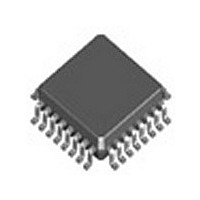
IC FANOUT BUFFER LV 3GHZ 32-LQFP
Manufacturer
IDT, Integrated Device Technology Inc
Type
Fanout Buffer (Distribution), Multiplexerr
Series
100ESr
Datasheet
1.MC100ES6111ACR2.pdf
(11 pages)
Specifications of MC100ES6111AC
Number Of Circuits
1
Ratio - Input:output
2:10
Differential - Input:output
Yes/Yes
Input
ECL, HSTL, PECL
Output
ECL, PECL
Frequency - Max
3GHz
Voltage - Supply
2.375 V ~ 3.465 V
Operating Temperature
-40°C ~ 110°C
Mounting Type
Surface Mount
Package / Case
32-LQFP
Frequency-max
2.7GHz
Number Of Clock Inputs
2
Mode Of Operation
Differential
Output Frequency
2700MHz
Output Logic Level
ECL/PECL
Operating Supply Voltage (min)
-2.375/2.375V
Operating Supply Voltage (typ)
-2.5/-3.3/2.5/3.3V
Operating Supply Voltage (max)
-3.465/3.465V
Package Type
TQFP
Operating Temp Range
0C to 110C
Operating Temperature Classification
Commercial
Signal Type
ECL/HSTL/PECL
Mounting
Surface Mount
Pin Count
32
Quiescent Current
100mA
Lead Free Status / RoHS Status
Lead free / RoHS Compliant
Available stocks
Company
Part Number
Manufacturer
Quantity
Price
Company:

Part Number:
MC100ES6111AC
Manufacturer:
ON
Quantity:
444
Company:
Part Number:
MC100ES6111AC
Manufacturer:
IDT
Quantity:
465
Company:
Part Number:
MC100ES6111AC
Manufacturer:
IDT, Integrated Device Technology Inc
Quantity:
10 000
Part Number:
MC100ES6111AC
Manufacturer:
MOTOROLA/摩托罗拉
Quantity:
20 000
Company:
Part Number:
MC100ES6111ACR2
Manufacturer:
IDT, Integrated Device Technology Inc
Quantity:
10 000


MPC100ES6111 Data Sheet
MPC100ES6111 REVISION 6 OCTOBER 1, 2009
CLK_SEL
CLKA
CLKA
CLKB
CLKB
Table 2. Function Table
Table 1. Pin Configuration
CLKA, CLKA
CLKB, CLKB
CLK_SEL
Q[0–9], Q[0–9]
V
V
V
1. In ECL mode (negative power supply mode), V
Figure 1. MC100ES6111 Logic Diagram
EE
CC
BB
power supply mode), V
referenced to the most positive supply (V
(1)
CLK_SEL
V
V
Control
CC
CC
Pin
0
1
Input
Input
Input
Output
Supply
Supply
Output
EE
is connected to GND (0 V) and V
Default
I/O
0
CC
V
Q0
Q0
Q1
Q1
Q2
Q2
Q3
Q3
Q4
Q4
Q5
Q5
Q6
Q6
Q7
Q7
Q8
Q8
Q9
Q9
BB
).
CLKA, CLKA input pair is active. CLKA can be
driven by ECL or PECL compatible signals.
ECL/PECL
HSTL/PECL
ECL/PECL
ECL/PECL
DC
EE
is either –3.3 V or –2.5 V and V
Type
V
V
Q2
Q2
Q1
Q1
Q0
Q0
CC
CC
CC
is either +3.3 V or +2.5 V. In both modes, the input and output levels are
Differential reference clock signal input
Alternative differential reference clock signal input
Active clock input select
Differential clock outputs
Negative power supply
Positive power supply. All V
power supply for correct DC and AC operation.
Reference voltage output for single ended ECL or PECL operation
2
0
Figure 2. 32-Lead Package Pinout (Top View)
LOW VOLTAGE 2.5V/3.3V DIFFERENTIAL ECL/PECL/HSTL FANOUT BUFFER
25
26
27
28
29
30
31
32
24
1
23
2
CC
MC100ES6111
22
3
is connected to GND (0 V). In PECL mode (positive
21
4
CLKB, CLKB input pair is active. CLKB can be
driven by HSTL or PECL compatible signals.
CC
20
5
Function
pins must be connected to the positive
19
6
18
7
©2009 Integrated Device Technology, Inc.
17
8
1
16
15
14
13
12
11
10
9
V
Q7
Q7
Q8
Q8
Q9
Q9
V
CC
CC
Related parts for MC100ES6111AC
Image
Part Number
Description
Manufacturer
Datasheet
Request
R

Part Number:
Description:
MICROCOUPLER, SMALL TRANSISTOR OUTPUT
Manufacturer:
Micropac Industries, Inc.
Part Number:
Description:
Steckbare Anschlussklemmen, Raster 5,08 mm
Manufacturer:
LUMBERG [Lumberg]
Datasheet:

Part Number:
Description:
MC100-50805K
Manufacturer:
Cooper/Bussmann
Datasheet:

Part Number:
Description:
TRANSLATION DEVICE DPI 80-PQFP
Manufacturer:
IDT, Integrated Device Technology Inc
Datasheet:
Part Number:
Description:
IDT PART
Manufacturer:
IDT, Integrated Device Technology Inc
Datasheet:
Part Number:
Description:
IC LIU T1/E1/J1 OCTAL 256PBGA
Manufacturer:
IDT, Integrated Device Technology Inc
Datasheet:

Part Number:
Description:
IC FREQ TIMING GENERATOR 28TSSOP
Manufacturer:
IDT, Integrated Device Technology Inc
Datasheet:
Part Number:
Description:
IC CLK DVR PLL 1:10 40VFQFPN
Manufacturer:
IDT, Integrated Device Technology Inc
Datasheet:
Part Number:
Description:
IC CLK FANOUT BUFFER 1:18 32LQFP
Manufacturer:
IDT, Integrated Device Technology Inc
Datasheet:
Part Number:
Description:
IC CLK FANOUT BUFFER 1:18 32LQFP
Manufacturer:
IDT, Integrated Device Technology Inc
Datasheet: