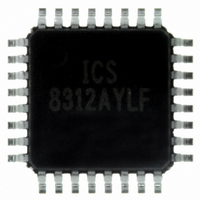
ICS8312AYLF IDT, Integrated Device Technology Inc, ICS8312AYLF Datasheet - Page 2

ICS8312AYLF
Manufacturer Part Number
ICS8312AYLF
Description
IC FANOUT BUFFER 1:12 32-LQFP
Manufacturer
IDT, Integrated Device Technology Inc
Series
HiPerClockS™r
Type
Fanout Buffer (Distribution)r
Datasheet
1.ICS8312AYLFT.pdf
(18 pages)
Specifications of ICS8312AYLF
Number Of Circuits
1
Ratio - Input:output
1:12
Differential - Input:output
No/No
Input
LVCMOS, LVTTL
Output
LVCMOS, LVTTL
Frequency - Max
250MHz
Voltage - Supply
1.6 V ~ 3.465 V
Operating Temperature
0°C ~ 85°C
Mounting Type
Surface Mount
Package / Case
32-LQFP
Frequency-max
250MHz
Number Of Outputs
12
Operating Supply Voltage (max)
3.465V
Operating Temp Range
0C to 85C
Propagation Delay Time
4.8ns
Operating Supply Voltage (min)
1.6V
Mounting
Surface Mount
Pin Count
32
Operating Supply Voltage (typ)
1.8/2.5/3.3V
Package Type
TQFP
Duty Cycle
55%
Operating Temperature Classification
Commercial
Lead Free Status / RoHS Status
Lead free / RoHS Compliant
Other names
800-1111
8312AYLF
8312AYLF
Available stocks
Company
Part Number
Manufacturer
Quantity
Price
Company:
Part Number:
ICS8312AYLF
Manufacturer:
IDT
Quantity:
277
Company:
Part Number:
ICS8312AYLF
Manufacturer:
IDT, Integrated Device Technology Inc
Quantity:
10 000
Company:
Part Number:
ICS8312AYLFT
Manufacturer:
IDT
Quantity:
300
Company:
Part Number:
ICS8312AYLFT
Manufacturer:
IDT, Integrated Device Technology Inc
Quantity:
10 000
Table 1. Pin Descriptions
NOTE: Pullup and Pulldown refer to internal input resistors. See Table 2, Pin Characteristics, for typical values.
Table 2. Pin Characteristics
IDT™ / ICS™ LVCMOS/LVTTL FANOUT BUFFER
Symbol
C
R
R
C
R
1, 5, 8, 12, 16,
18, 20, 22, 24,
10, 14, 19, 23,
ICS8312
LOW SKEW, 1-TO-12 LVCMOS/LVTTL FANOUT BUFFER
17, 21, 25, 29
26, 28, 30, 32
9, 11, 13, 15,
IN
PULLUP
PULLDOWN
PD
OUT
Number
27, 31
2, 7
3
4
6
Parameter
Input Capacitance
Input Pullup Resistor
Input Pulldown Resistor
Power Dissipation Capacitance
(per output)
Output Impedance
Q11, Q10, Q9, Q8,
Q7, Q6, Q5, Q4,
Q3, Q2, Q1, Q0
CLK_EN
Name
V
GND
CLK
V
OE
DDO
DD
Output
Power
Power
Power
Input
Input
Input
Type
Pulldown
Pullup
Pullup
V
V
V
Test Conditions
DDO
DDO
DDO
V
V
DDO
DDO
V
DDO
= 1.8V ± 0.2V
Description
Power supply ground.
Positive supply pins.
Synchronous control for enabling and disabling clock outputs.
LVCMOS / LVTTL interface levels.
Single-ended clock input. LVCMOS/LVTTL interface levels.
Output enable. Controls enabling and disabling of outputs Q[0:11].
LVCMOS / LVTTL interface levels.
Single-ended clock outputs. LVCMOS/LVTTL interface levels.
Output supply pins.
= 3.3V ± 5%
= 2.5V ± 5%
2
= 3.465V
= 2.625V
= 2V
Minimum
Typical
51
51
10
4
7
7
ICS8312AY REV. D JULY 3, 2008
Maximum
19
18
16
Units
k
k
pF
pF
pF
pF
Ω
Ω
Ω
Ω
Ω


