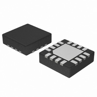
NBSG14MNG ON Semiconductor, NBSG14MNG Datasheet - Page 3

NBSG14MNG
Manufacturer Part Number
NBSG14MNG
Description
IC DRIVER CLOCK RSECL 1:4 16QFN
Manufacturer
ON Semiconductor
Type
Fanout Buffer (Distribution), Datar
Datasheet
1.NBSG14MNR2G.pdf
(13 pages)
Specifications of NBSG14MNG
Number Of Circuits
1
Ratio - Input:output
1:4
Differential - Input:output
Yes/Yes
Input
CML, LVCMOS, LVDS, LVTTL, NECL, PECL, RSECL
Output
RSECL, RSNECL, RSPECL
Frequency - Max
12GHz
Voltage - Supply
2.375 V ~ 3.465 V
Operating Temperature
-40°C ~ 85°C
Mounting Type
Surface Mount
Package / Case
16-TFQFN Exposed Pad
Frequency-max
12GHz
Number Of Outputs
8
Operating Supply Voltage (max)
-3.465/3.465V
Operating Temp Range
-40C to 85C
Propagation Delay Time
0.16ns
Operating Supply Voltage (min)
-2.375/2.375V
Mounting
Surface Mount
Pin Count
16
Operating Supply Voltage (typ)
-2.5/-3.3/2.5/3.3V
Package Type
QFN EP
Input Frequency
12GHz
Operating Temperature Classification
Industrial
Clock Ic Type
Clock Driver
Frequency
12GHz
No. Of Outputs
4
Supply Current
60mA
Supply Voltage Range
2.375V To 3.465V
Digital Ic Case Style
QFN
No. Of Pins
16
Rohs Compliant
Yes
Lead Free Status / RoHS Status
Lead free / RoHS Compliant
Other names
NBSG14MNGOS
Available stocks
Company
Part Number
Manufacturer
Quantity
Price
Company:
Part Number:
NBSG14MNG
Manufacturer:
ON Semiconductor
Quantity:
1
Part Number:
NBSG14MNG
Manufacturer:
ON/安森美
Quantity:
20 000
Table 2. INTERFACING OPTIONS
Table 3. ATTRIBUTES
1. For additional information, see Application Note AND8003/D.
Internal Input Pulldown Resistor (CLK, CLK)
Internal Input Pullup Resistor (CLK)
ESD Protection
Moisture Sensitivity (Note 1)
Flammability Rating
Transistor Count
Meets or exceeds JEDEC Spec EIA/JESD78 IC Latchup Test
VTCLK
VTCLK
INTERFACING OPTIONS
CLK
CLK
RSECL, PECL, NECL
LVTTL, LVCMOS
AC−COUPLED
50 W
50 W
LVDS
CML
Characteristics
75 KW
Figure 3. Logic Diagram
http://onsemi.com
V
V
Oxygen Index: 28 to 34
CC
EE
75 KW
Human Body Model
36.5 KW
Machine Model
3
An External Voltage (V
1.5 V for LVTTL and V
the Unused Differential Input. Nominal V
FCBGA−16
Standard ECL Termination Techniques
Connect VTCLK and VTCLK Together
Bias VTCLK and VTCLK Inputs within
This Voltage must be within the V
Connect VTCLK and VTCLK to V
QFN−16
Common Mode Range (V
CONNECTIONS
Specification.
Pb Pkg
Level 3
Level 1
Value
UL 94 V−0 @ 0.125 in
THR
CC
/2 for LVCMOS Inputs.
) should be Applied to
36.5 kW
> 100 V
> 2 kV
75 kW
158
IHCMR
Pb−Free Pkg
Level 3
Level 1
Value
Q3
Q3
Q2
Q2
Q1
Q1
Q0
Q0
THR
CC
)
THR
is


