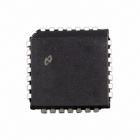
CGS2535TV National Semiconductor, CGS2535TV Datasheet - Page 5

CGS2535TV
Manufacturer Part Number
CGS2535TV
Description
IC CLOCK DVR IND QUAD 1-4 28PLCC
Manufacturer
National Semiconductor
Type
Fanout Buffer (Distribution)r
Datasheet
1.CGS2535TV.pdf
(7 pages)
Specifications of CGS2535TV
Number Of Circuits
1
Ratio - Input:output
4:16
Differential - Input:output
No/No
Input
CMOS
Output
CMOS
Frequency - Max
125MHz
Voltage - Supply
3 V ~ 5.25 V
Operating Temperature
-40°C ~ 85°C
Mounting Type
Surface Mount
Package / Case
28-PLCC
Frequency-max
125MHz
Lead Free Status / RoHS Status
Contains lead / RoHS non-compliant
Other names
*CGS2535TV
Available stocks
Company
Part Number
Manufacturer
Quantity
Price
Company:
Part Number:
CGS2535TV
Manufacturer:
KEC
Quantity:
694
Part Number:
CGS2535TV
Manufacturer:
NS/国半
Quantity:
20 000
Company:
Part Number:
CGS2535TVX
Manufacturer:
Texas Instruments
Quantity:
10 000
CGS2534/35/36/37
MEMORY ARRAY DRIVING
In order to minimize the total load on the address bus, quite
often memory arrays are driven by buffers while having the
inputs of the buffers tied together. Although this practice was
feasible in the conventional memory designs, in today’s high
speed, large buswidth designs which require address fetch-
ing at higher speeds, this technique produces many undes-
ired results such as cross-talk and over/undershoot.
CGS2534/35/36/37 Quad 1 to 4 clock drivers were designed
specifically to address these application issues on high
speed, large memory arrays systems.
These drivers are optimized to drive large loads, with 3.5 ns
propagation delays. These drivers produce less noise while
reducing the total capacitive loading on the address bus by
having only four inputs tied together (see the diagram below,
point A). This helps to minimize the overshoot and under-
shoot by having only four outputs being switched simulta-
neously.
Device
2534
2535
2536
2537
3 or 5
3 or 5
V
5
5
CC
CMOS
CMOS
TTL
TTL
I/O
5
Inverting quad 1–4
Non-inverting quad 1–4
Inverting, Non-inverting, ÷2
Inverting quad 1–4 with series 8Ω output resistors
Also this larger fan-out helps to save board space since for
every one of these drivers, two conventional buffers were
typically being used.
Another feature associated with these clock drivers is a
350 ps pin-to-pin skew specification. The minimum skew
specification allows high speed memory system designers to
optimize the performance of their memory sub-system by
operating at higher frequencies without having concerns
about output-to-output (bank-to-bank) synchronization prob-
lems which are associated with driving high capacitive loads
(Point B).
The diagram below depicts a “2534/35/36/37” a memory
subsystem operating at high speed with large memory ca-
pacity. The address bus is common to both the memory and
the CPU and I/Os.
These drivers can operate beyond 125 MHz, and are also
available in 3V–5V TTL/CMOS versions with large current
drive .
Output Configuration
01195408
www.national.com


