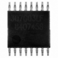
ICS307G-03LFT IDT, Integrated Device Technology Inc, ICS307G-03LFT Datasheet - Page 7

ICS307G-03LFT
Manufacturer Part Number
ICS307G-03LFT
Description
IC CLOCK SOURCE PROGR 16-TSSOP
Manufacturer
IDT, Integrated Device Technology Inc
Type
Clock Generatorr
Datasheet
1.ICS307G-03LFT.pdf
(14 pages)
Specifications of ICS307G-03LFT
Pll
Yes
Input
Clock, Crystal
Output
LVCMOS
Number Of Circuits
1
Ratio - Input:output
2:3
Differential - Input:output
No/No
Frequency - Max
270MHz
Divider/multiplier
Yes/No
Voltage - Supply
3 V ~ 3.6 V
Operating Temperature
0°C ~ 70°C
Mounting Type
Surface Mount
Package / Case
16-TSSOP
Frequency-max
270MHz
Lead Free Status / RoHS Status
Lead free / RoHS Compliant
Other names
307G-03LFT
800-1796-2
800-1796-2
Table 8. Miscellaneous Control Bits
External Components
The ICS307-03 requires a minimum number of external components for proper operation.
Decoupling Capacitors
TheICS307-03 requires 0.01 F decoupling capacitors to be connected between each VDD pin and the Ground Plane. The
0.01 F capacitors must be placed as close to the ICS307-03’s power pins as possible to minimize lead inductance.
Output Termination
The ICS307-03 has advanced output pads that allows the device to achieve very high speed (270 MHz) operation with single
ended clock outputs. The clock outputs on the ICS307-03 are designed to be directly connected to a 50 Ohm transmission
line without the need for any series resistors.
Crystal Selection
A parallel resonant, fundamental mode crystal with a load
(correlation) capacitance of 12 pF should be used. For
crystals with a specified load capacitance greater than 12
pF, additional crystal capacitors may be connected from
For a single ended clock input, connect it to X1 and leave X2 unconnected with no capacitors on either pin.
Initial Output Frequency
ICS307-03 on-chip registers are initially configured to
provide a 1x output clock on the CLK1 output, and 0.5x clock
on CLK2 and CLK3. The output frequency will be the same
as the input clock or crystal for input frequencies from 10 -
50 MHz. This is useful when the ICS307-03 needs to
provide an initial system clock at power-up.
IDT® SERIALLY PROGRAMMABLE CLOCK SOURCE
ICS307-03
SERIALLY PROGRAMMABLE CLOCK SOURCE
24~88
110
111
112
122
123
124
125
126
129
130
131
Bit
Function
Reserved—set to 0
OE1—set to 1 to enable CLK1
OE2—set to 1 to enable CLK2
1 = Normal Operation, 0 = power down feedback counter, charge pump and VCO
Crystal Input = 1, Clock Input = 0
Selects source for CLK2 (see block diagram)
Selects source for CLK3 (see block diagram)
Reserved—set to 0
Reserved—set to 0
OE3—set to 1 to enable CLK3
Reserved—set to 0
Reserved—set to 0
7
each of the pins X1 and X2 to ground as shown in the Block
Diagram on page 1. The value (in pF) of these crystal caps
should be = (C
capacitance in pF.
L
-12)*2, where C
SER PROG CLOCK SYNTHESIZER
L
is the crystal load
ICS307-03
REV L 032911


