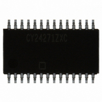
CY24271ZXC Cypress Semiconductor Corp, CY24271ZXC Datasheet - Page 11

CY24271ZXC
Manufacturer Part Number
CY24271ZXC
Description
IC CLOCK GEN XDR 28-TSSOP
Manufacturer
Cypress Semiconductor Corp
Type
Clock Generator, Fanout Distributionr
Series
Rambus™, XDR™r
Datasheet
1.CY24271ZXC.pdf
(16 pages)
Specifications of CY24271ZXC
Number Of Circuits
1
Package / Case
28-TSSOP
Pll
Yes with Bypass
Input
Clock
Output
Clock
Ratio - Input:output
1:4
Differential - Input:output
Yes/Yes
Frequency - Max
1.067MHz
Divider/multiplier
No/Yes
Voltage - Supply
2.375 V ~ 2.625 V
Operating Temperature
0°C ~ 70°C
Mounting Type
Surface Mount
Frequency-max
800MHz
Minimum Input Frequency
133 MHz, 100 MHz
Output Frequency Range
300 MHz to 800 MHz
Supply Voltage (max)
2.625 V
Supply Voltage (min)
2.375 V
Maximum Operating Temperature
+ 70 C
Minimum Operating Temperature
0 C
Mounting Style
SMD/SMT
Operating Supply Voltage
2.5 V
Lead Free Status / RoHS Status
Lead free / RoHS Compliant
Lead Free Status / RoHS Status
Lead free / RoHS Compliant, Lead free / RoHS Compliant
Other names
428-2218-5
CY24271ZXC
CY24271ZXC
Available stocks
Company
Part Number
Manufacturer
Quantity
Price
Company:
Part Number:
CY24271ZXC
Manufacturer:
Maxim
Quantity:
12
Example External Resistor Values
and Termination Voltages for a 50 Channel
Signal Waveforms
A physical signal that appears at the pins of a device is deemed
valid or invalid depending on its voltage and timing relations with
other signals. Input and output voltage waveforms are defined as
shown in
Document Number: 001-00411 Rev. *C
Parameter
Figure
R
V
R
R
R
R
V
RC
TS
T
T
1
2
3
4. Both rise and fall times are defined between
CLKB
CLK
V
(t)
Value
2.5V
1.2V
39.2
66.5
93.1
49.9
200
Figure 4. Input and Output Waveforms
Figure 5. Crossing Point Voltage
Unit
V
V
t
F
the 20% and 80% points of the voltage swing, with the swing
defined as V
Figure 5
nominal crossing point between the complementary outputs is
defined as the 50% point of the DC voltage levels. There are two
crossing points defined: Vx+ at the rising edge of CLK and Vx–
at the falling edge of CLK. For some waveforms, both Vx+ and
Vx– are below Vx,nom (for example, if t
Jitter
This section defines the specifications that relate to timing
uncertainty (or jitter) of the input and output waveforms.
on page 12
respect to the falling edge of the CLK signal. Cycle-to-cycle jitter
is the difference between cycle times of adjacent cycles. Equal
requirements apply rising edges of the CLK signal.
page 12
(t
between t
Equal requirements apply to t
click cycles.
DC,ERR
). Cycle-to-cycle duty cycle is defined as the difference
t
shows the definition of the output crossing point. The
R
shows the definition of cycle-to-cycle duty cycle error
PW+
H
shows the definition of cycle-to-cycle jitter with
–V
(high times) of adjacent differential clock cycles.
L
.
Vx+
Vx.nom
Vx-
8 0 %
V
2 0 %
V
H
L
PW-
, low times of the differential
CR
is larger than t
CY24271
Page 11 of 16
Figure 7 on
Figure 6
CF
).
[+] Feedback


