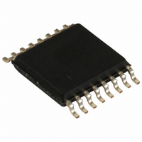
CY22394FXI Cypress Semiconductor Corp, CY22394FXI Datasheet - Page 9

CY22394FXI
Manufacturer Part Number
CY22394FXI
Description
IC CLOCK GEN PROG 16-TSSOP
Manufacturer
Cypress Semiconductor Corp
Type
Clock Generator, Fanout Distributionr
Datasheet
1.CY22394FXC.pdf
(19 pages)
Specifications of CY22394FXI
Number Of Circuits
1
Package / Case
16-TSSOP
Pll
Yes
Input
Crystal
Output
CMOS, PECL
Ratio - Input:output
1:5
Differential - Input:output
No/Yes
Frequency - Max
166MHz, 375MHz
Divider/multiplier
Yes/No
Voltage - Supply
3.135 V ~ 3.465 V
Operating Temperature
-40°C ~ 85°C
Mounting Type
Surface Mount
Frequency-max
375MHz
Maximum Input Frequency
150 MHz
Minimum Input Frequency
1 MHz
Output Frequency Range
125 MHz to 375 MHz
Supply Voltage (max)
3.465 V
Supply Voltage (min)
3.135 V
Maximum Operating Temperature
+ 85 C
Minimum Operating Temperature
- 40 C
Mounting Style
SMD/SMT
Operating Supply Voltage
3.3 V
Lead Free Status / RoHS Status
Lead free / RoHS Compliant
For Use With
428-1918 - KIT DEV FTG PROGRAMMING KIT428-1455 - SOCKET ADAPTER FOR CY2239X
Lead Free Status / Rohs Status
Lead free / RoHS Compliant
Other names
428-2181-5
CY22394FXI
CY22394FXI
Available stocks
Company
Part Number
Manufacturer
Quantity
Price
Company:
Part Number:
CY22394FXI
Manufacturer:
ADI
Quantity:
36
Document #: 38-07186 Rev. *B
Read Operations
Read operations are initiated the same way as Write opera-
tions except that the R/W bit of the slave address is set to ‘1’
(HIGH). There are three basic read operations: current
address read, random read, and sequential read.
Current Address Read
The CY22393,CY22394 and CY22395 has an onboard
address counter that retains 1 more than the address of the
last word access. If the last word written or read was word ‘n’,
then a current address read operation would return the value
stored in location ‘n+1’. When the CY22393,CY22394 and
CY22395 receives the slave address with the R/W bit set to a
‘1’, the CY22393,CY22394 and CY22395 issues an
acknowledge and transmits the 8-bit word. The master device
does not acknowledge the transfer, but does generate a STOP
condition, which causes the CY22393,CY22394 and CY22395
to stop transmission.
Random Read
Through random read operations, the master may access any
memory location. To perform this type of read operation, first
the word address must be set. This is accomplished by
sending the address to the CY22393,CY22394 and CY22395
as part of a write operation. After the word address is sent, the
SDAT
SCL
START
Condition
Figure 1. Data Transfer Sequence on the Serial Bus
Address or
Acknowledge
Valid
Data may
be changed
master
acknowledge. This terminates the write operation before any
data is stored in the address, but not before the internal
address pointer is set. Next the master reissues the control
byte with the R/W byte set to ‘1’. The CY22393,CY22394 and
CY22395 then issues an acknowledge and transmits the 8-bit
word. The master device does not acknowledge the transfer,
but does generate a STOP condition which causes the
CY22393,CY22394 and CY22395 to stop transmission.
Sequential Read
Sequential read operations follow the same process as
random reads except that the master issues an acknowledge
instead of a STOP condition after transmission of the first 8-bit
data word. This action results in an incrementing of the internal
address pointer, and subsequently output of the next 8-bit data
word. By continuing to issue acknowledges instead of STOP
conditions, the master may serially read the entire contents of
the slave device memory. Note that register addresses outside
of 08H to 1BH and 40H to 57H can be read from but are not
real registers and do not contain configuration information.
When the internal address pointer points to the FFH register,
after the next increment, the pointer will point to the 00H
register.
generates
a
STOP
Condition
START
condition
CY22393
CY22394
CY22395
following
Page 9 of 19
the


