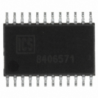
ICS87004AGLF IDT, Integrated Device Technology Inc, ICS87004AGLF Datasheet - Page 2

ICS87004AGLF
Manufacturer Part Number
ICS87004AGLF
Description
IC CLK GENERATOR ZD 1:4 24-TSSOP
Manufacturer
IDT, Integrated Device Technology Inc
Series
HiPerClockS™r
Type
Clock Generator, Fanout Distribution, Multiplexer , Zero Delay Bufferr
Datasheet
1.ICS87004AGLF.pdf
(15 pages)
Specifications of ICS87004AGLF
Pll
Yes with Bypass
Input
HCSL, LVDS, LVHSTL, LVPECL, SSTL
Output
LVCMOS, LVTTL
Number Of Circuits
1
Ratio - Input:output
2:4
Differential - Input:output
Yes/No
Frequency - Max
250MHz
Divider/multiplier
Yes/Yes
Voltage - Supply
2.375 V ~ 3.465 V
Operating Temperature
0°C ~ 70°C
Mounting Type
Surface Mount
Package / Case
24-TSSOP
Frequency-max
250MHz
Lead Free Status / RoHS Status
Lead free / RoHS Compliant
Other names
800-1192
800-1192-5
800-1192
87004AGLF
800-1192-5
800-1192
87004AGLF
Available stocks
Company
Part Number
Manufacturer
Quantity
Price
Company:
Part Number:
ICS87004AGLF
Manufacturer:
IDT Integrated Device Technolo
Quantity:
135
Company:
Part Number:
ICS87004AGLF
Manufacturer:
IDT
Quantity:
91
ICS87004 Data Sheet
Table 1. Pin Descriptions
NOTE: Pullup and Pulldown refer to internal input resistors. See Table 2, Pin Characteristics, for typical values.
Table 2. Pin Characteristics
ICS87004AG REVISION C DECEMBER 1, 2009
Symbol
C
R
R
C
R
OUT
IN
PULLUP
PULLDOWN
PD
1, 12, 21
3, 19, 23
Number
22, 24
2, 20,
4, 5,
6, 7
10
11
13
14
15
16
17
18
8
9
Parameter
Input Capacitance
Input Pullup Resistor
Input Pulldown Resistor
Power Dissipation
Capacitance (per output)
Output Impedance
SEL0, SEL1,
SEL2, SEL3
CLK_SEL
PLL_SEL
Q0, Q3,
Q2, Q1
nCLK0
nCLK1
FB_IN
Name
V
CLK0
CLK1
V
GND
V
MR
DDO
DDA
DD
Output
Power
Power
Power
Power
Input
Input
Input
Input
Input
Input
Input
Input
Input
Type
Pulldown
Pulldown
Pulldown
Pulldown
Pulldown
Pulldown
Pulldown
Pulldown
Pullup/
Pullup/
Pullup
V
V
DD
DD
Test Conditions
Description
Power supply ground.
Single-ended clock outputs. 7
LVCMOS/LVTTL interface levels.
Output supply pins.
Determines output divider values in Table 3. LVCMOS / LVTTL interface levels.
Clock select input. When HIGH, selects differential CLK1, nCLK1. When LOW,
selects differential CLK0, nCLK0. LVCMOS/LVTTL interface levels.
Core supply pin.
Non-inverting differential clock input.
Inverting differential clock input. V
Analog supply pin.
Inverting differential clock input. V
Non-inverting differential clock input.
PLL select. Selects between the PLL and reference clock as the input to the
dividers. When LOW, selects the reference clock (PLL Bypass). When HIGH,
selects PLL (PLL Enabled). LVCMOS/LVTTL interface levels.
Feedback input to phase detector for regenerating clocks with “Zero Delay.”
Connect to one of the outputs. LVCMOS/LVTTL interface levels.
Active HIGH Master Reset. When logic HIGH, the internal dividers are reset
causing the outputs to go low. When logic LOW, the internal dividers and the
outputs are enabled. LVCMOS / LVTTL interface levels.
, V
, V
DDO
DDO
= 3.465V
= 2.625V
2
1:4, DIFFERENTIAL-TO-LVCMOS/LVTTL ZERO DELAY CLOCK GENERATOR
Ω
Minimum
typical output impedance.
DD
DD
/2 default when left floating.
/2 default when left floating.
5
Typical
©2009 Integrated Device Technology, Inc.
51
51
4
7
Maximum
12
23
17
Units
k
k
pF
pF
pF
Ω
Ω
Ω


