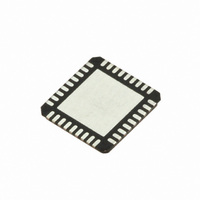
SI5317A-C-GM Silicon Laboratories Inc, SI5317A-C-GM Datasheet - Page 13

SI5317A-C-GM
Manufacturer Part Number
SI5317A-C-GM
Description
IC CLK JITTER CLEANR PROG 36QFN
Manufacturer
Silicon Laboratories Inc
Type
Jitter Cleanerr
Series
Si5317r
Datasheet
1.SI5317C-C-GM.pdf
(46 pages)
Specifications of SI5317A-C-GM
Package / Case
36-QFN
Pll
Yes with Bypass
Input
Clock, Crystal
Output
CML, CMOS, LVDS, LVPECL
Number Of Circuits
1
Ratio - Input:output
1:2
Differential - Input:output
Yes/Yes
Frequency - Max
710MHz
Divider/multiplier
No/No
Voltage - Supply
1.71 V ~ 3.63 V
Operating Temperature
-40°C ~ 85°C
Mounting Type
Surface Mount
Frequency-max
710MHz
Termination Style
SMD/SMT
Output Format
LVPECL
Dimensions
5 mm W x 7 mm L x 1.85 mm H
Minimum Operating Temperature
- 40 C
Maximum Operating Temperature
+ 85 C
Mounting Style
SMD/SMT
Product
XO
Frequency
10 MHz to 945 MHz
Frequency Stability
+/- 20 PPM
Supply Voltage
3.3 Volts
Height
1.85 mm
Lead Free Status / RoHS Status
Lead free / RoHS Compliant
Lead Free Status / RoHS Status
Lead free / RoHS Compliant, Lead free / RoHS Compliant
Other names
336-1923
Table 6. Thermal Characteristics
(V
Table 7. Absolute Maximum Limits
Thermal Resistance
Junction to Ambient
Thermal Resistance
Junction to Case
DC Supply Voltage
LVCMOS Input Voltage
CKINn Voltage Level Limits
XA/XB Voltage Level Limits
Operating Junction Temperature
Storage Temperature Range
ESD HBM Tolerance (100 pF, 1.5 kΩ); All pins except
CKIN+/CKIN–
ESD MM Tolerance; All pins except CKIN+/CKIN–
ESD HBM Tolerance (100 pF, 1.5 kΩ); CKIN+/CKIN–
ESD MM Tolerance; CKIN+/CKIN–
Latch-Up Tolerance
Note: Permanent device damage may occur if the Absolute Maximum Ratings are exceeded. Functional operation should be
DD
= 1.8 ±5%, 2.5 ±10%, or 3.3 V ±10%, T
restricted to the conditions as specified in the operation sections of this data sheet. Exposure to absolute maximum
rating conditions for extended periods of time may affect device reliability.
Parameter
Parameter
Symbol
JC
JA
A
= –40 to 85 ºC)
Test Condition
Still Air
Rev. 1.1
Symbol
CKN
XA
T
V
T
V
STG
JCT
DIG
DD
VIN
VIN
Min
—
—
–0.3 to (V
–0.5 to 3.8
–55 to 150
–55 to 150
0 to V
Typ
0 to 1.2
JESD78 Compliant
32
14
Value
150
750
100
2
DD
DD
+ 0.3)
Max
Si5317
—
—
Unit
kV
C
C
ºC/W
V
V
V
V
V
V
V
ºC/W
Unit
13


