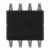
MB88154APNF-G-102-JNE1 Fujitsu Semiconductor America Inc, MB88154APNF-G-102-JNE1 Datasheet - Page 4

MB88154APNF-G-102-JNE1
Manufacturer Part Number
MB88154APNF-G-102-JNE1
Description
IC SSCG EMI RED 8-SOP
Manufacturer
Fujitsu Semiconductor America Inc
Type
Fanout Distribution, Spread Spectrum Clock Generatorr
Datasheet
1.MB88154APNF-G-102-JNE1.pdf
(20 pages)
Specifications of MB88154APNF-G-102-JNE1
Pll
Yes with Bypass
Input
CMOS
Output
CMOS
Number Of Circuits
1
Ratio - Input:output
1:2
Differential - Input:output
No/No
Frequency - Max
67MHz
Divider/multiplier
No/No
Voltage - Supply
3 V ~ 3.6 V
Operating Temperature
-40°C ~ 85°C
Mounting Type
Surface Mount
Package / Case
8-SOP
Frequency-max
67MHz
For Use With
865-1034 - BOARD EVALUATION FOR MB88154
Lead Free Status / RoHS Status
Lead free / RoHS Compliant
Other names
865-1041
Available stocks
Company
Part Number
Manufacturer
Quantity
Price
Company:
Part Number:
MB88154APNF-G-102-JNE1
Manufacturer:
TI
Quantity:
165
4
MB88154A
Preventing Latch-up
Handling unused pins
The attention when the external clock is used
Power supply pins
Oscillation circuit
HANDLING DEVICES
A latch-up can occur if, on this device, (a) a voltage higher than V
input or output pin or (b) a voltage higher than the rating is applied between V
if it occurs, significantly increases the power supply current and may cause thermal destruction of an element.
When you use this device, be very careful not to exceed the maximum rating.
Do not leave an unused input pin open, since it may cause a malfunction. Handle by, using a pull-up or
pull-down resistor.
Unused output pin should be opened.
Input the clock to XIN pin, and XOUT pin should be opened when you use the external clock.
Please pay attention so that an overshoot and an undershoot do not occur to an input clock of XIN pin.
Please design connecting the power supply pin of this device by as low impedance as possible from the current
supply source.
We recommend connecting electrolytic capacitor (about 10 µF) and the ceramic capacitor (about 0.01 µF) in
parallel between V
Noise near the XIN and XOUT pins may cause the device to malfunction. Design printed circuit boards so that
electric wiring of XIN or XOUT pin and the resonator do not intersect other wiring.
Design the printed circuit board that surrounds the XIN and XOUT pins with ground.
SS
pin and V
DD
pin near the device, as a bypass capacitor.
DD
or a voltage lower than V
DD
pin and V
SS
SS
pin. The latch-up,
is applied to an


