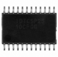
IDTCSP2510CPGG IDT, Integrated Device Technology Inc, IDTCSP2510CPGG Datasheet - Page 4

IDTCSP2510CPGG
Manufacturer Part Number
IDTCSP2510CPGG
Description
IC CLK DVR ZD BUFFER PLL 24TSSOP
Manufacturer
IDT, Integrated Device Technology Inc
Type
PLL Driver, Zero Delay Bufferr
Datasheet
1.IDTCSP2510CPG8.pdf
(9 pages)
Specifications of IDTCSP2510CPGG
Pll
Yes with Bypass
Input
Clock
Output
Clock
Number Of Circuits
1
Ratio - Input:output
1:10
Differential - Input:output
No/No
Frequency - Max
140MHz
Divider/multiplier
No/No
Voltage - Supply
3 V ~ 3.6 V
Operating Temperature
0°C ~ 85°C
Mounting Type
Surface Mount
Package / Case
24-TSSOP
Frequency-max
140MHz
Lead Free Status / RoHS Status
Lead free / RoHS Compliant
Other names
800-1706
800-1706-5
800-1706
CSP2510CPGG
800-1706-5
800-1706
CSP2510CPGG
Available stocks
Company
Part Number
Manufacturer
Quantity
Price
Company:
Part Number:
IDTCSP2510CPGG
Manufacturer:
ATHEROS
Quantity:
6 770
Part Number:
IDTCSP2510CPGG
Manufacturer:
IDT
Quantity:
20 000
DC ELECTRICAL CHARACTERISTICS OVER OPERATING FREE-AIR TEMPERA-
TURE RANGE
NOTES:
1. For Industrial devices, operating free-air temperature = -40°C to +85°C.
2. Time required for the integrated PLL circuit to obtain phase lock of its feedback signal to its reference signal. For phase lock to be obtained, a fixed-frequency, fixed-phase
NOTES:
1. For Industrial devices, operating free-air temperature = -40°C to +85°C.
2. For conditions shown as Min. or Max., use the appropriate value specified under recommended operating conditions.
3. For I
TIMING REQUIREMENTS OVER OPERATING RANGE OF SUPPLY VOLTAGE AND
OPERATING FREE-AIR TEMPERATURE
IDTCSP2510C
3.3V PHASE-LOCK LOOP CLOCK DRIVER
Symbol
reference signal must be present at CLK. Until phase lock is obtained, the specifications for propagation delay, skew, and jitter parameters given in the switching characteristics
table are not applicable.
I
ΔI
DDA
V
C
V
V
V
V
I
f
DD
CLOCK
OH
I
OL
PD
IK
IH
IL
DD
I
(3)
DD
of AV
Description
Input Clamp Voltage
Input HIGH Level
Input LOW Level
HIGH Level Output Voltage
LOW Level Output Voltage
Input Current
Supply Current
Change in Supply Current
Power Dissipation Capacitance
AV
DD
, see TYPICAL CHARACTERISTICS.
DD
Power Supply Current
(1)
Clock frequency
Input clock duty cycle
Stabilization time
(2)
Test Conditions
I
I
I
I
I
I
I
V
V
I
One input at V
I
OH
OH
OH
OL
OL
OL
O
I
I
= -18mA
= V
= V
= 0, Outputs: LOW or HIGH
= 100μA
= 12mA
= -100μA
= -12mA
= 6mA
= -6mA
DD
DD
or GND
or GND, AV
DD
- 0.6V, other inputs at V
DD
= GND,
(1)
4
DD
or GND
40%
Min.
⎯
25
AV
Min. to Max. V
Min. to Max.
3.3V to 3.6V
DD
3.6V
3.6V
3.6V
V
3V
⎯
⎯
3V
3V
3V
3V
DD
= 3.3V
0ºC TO 85ºC TEMPERATURE RANGE
DD
Min.
Max.
60%
2.1
2.4
⎯
⎯
⎯
⎯
⎯
⎯
⎯
⎯
⎯
⎯
140
2
– 0.2
1
Typ.
⎯
⎯
⎯
⎯
⎯
⎯
⎯
⎯
⎯
⎯
⎯
⎯
10
10
(2)
Max.
– 1.2
0.55
500
⎯
0.8
⎯
⎯
⎯
0.2
0.8
±5
⎯
10
14
MHz
Unit
ms
Unit
mA
μA
μA
μA
pF
V
V
V
V
V


