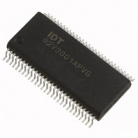
IDT82V3001APVG IDT, Integrated Device Technology Inc, IDT82V3001APVG Datasheet - Page 16

IDT82V3001APVG
Manufacturer Part Number
IDT82V3001APVG
Description
IC PLL WAN W/SGL REF INP 56-SSOP
Manufacturer
IDT, Integrated Device Technology Inc
Type
PLL Clock Generatorr
Series
-r
Datasheet
1.IDT82V3001APVG8.pdf
(28 pages)
Specifications of IDT82V3001APVG
Input
CMOS, TTL
Output
CMOS, TTL
Frequency - Max
32.768MHz
Voltage - Supply
3 V ~ 3.6 V
Operating Temperature
-40°C ~ 85°C
Mounting Type
Surface Mount
Package / Case
56-SSOP
Frequency-max
32.768MHz
Function
Wan PLL
Operating Temperature (max)
85C
Operating Temperature (min)
-40C
Package Type
SSOP
Pin Count
56
Mounting
Surface Mount
Lead Free Status / RoHS Status
Lead free / RoHS Compliant
Lead Free Status / RoHS Status
Compliant, Lead free / RoHS Compliant
Other names
82V3001APVG
Available stocks
Company
Part Number
Manufacturer
Quantity
Price
Company:
Part Number:
IDT82V3001APVG
Manufacturer:
MARVELL
Quantity:
12 000
Company:
Part Number:
IDT82V3001APVG
Manufacturer:
IDT
Quantity:
2
Part Number:
IDT82V3001APVG
Manufacturer:
IDT
Quantity:
20 000
3.9
required to minimize supply noise modulation of the output clocks. The
common sources of power supply noise are switching power supplies
and the high switching noise from the outputs to the internal PLL. The
82V3001A provides separate power pins: V
are for the internal analog PLL, and V
well as I/O driver circuits.
switching regulator, the power supply output should be filtered with
sufficient bulk capacity to minimize ripple and 0.1 uF (0402 case size,
ceramic) capacitors to filter out the switching transients.
individually. V
power supply plane through vias, and bypass capacitors should be used
FUNCTIONAL DESCRIPTION
IDT82V3001A
To achieve optimum jitter performance, power supply filtering is
To minimize switching power supply noise generated by the
For the 82V3001A, the decoupling for V
POWER SUPPLY FILTERING TECHNIQUES
DDD
and V
3.3 V
3.3 V
DDA
SLF7028T-100M1R1
SLF7028T-100M1R1
should be individually connected to the
DDD
pins are for the core logic as
DDA
DDA
10 µF
10 µF
Figure - 11 IDT82V3001A Power Decoupling Scheme
and V
and V
DDD
DDD
. V
are handled
DDA
pins
0.1 µF
0.1 µF
0.1 µF
0.1 µF
0.1 µF
16
48
19
26
37
13
for each pin.
bead should be connected to each power pin.
can be achieved by using one 10 uF (1210 case size, ceramic) and at
least two 0.1 uF (0402 case size, ceramic) capacitors in parallel. The 0.1
uF (0402 case size, ceramic) capacitors must be placed next to the
V
be of 1210 case size, and it must be ceramic for lowest possible ESR
(Effective Series Resistance). The 0.1 uF should be of case size 0402,
which offers the lowest ESL (Effective Series Inductance) to achieve low
impedance towards the high speed range.
uF (1210 case size, ceramic) capacitors are recommended. The 0.1 uF
capacitors should be placed as close to the V
V
V
V
V
V
DDA
DDA
DDA
DDD
DDD
DDD
The analog power supply V
For V
Please refer to evaluation board schematic for details.
pins and as close as possible. Note that the 10 uF capacitor must
IDT82V3001A
DDD
, at least three 0.1 uF (0402 case size, ceramic) and one 10
Figure - 11
WAN PLL WITH SINGLE REFERENCE INPUT
V
V
V
V
V
SS
SS
SS
SS
SS
illustrates how bypass capacitor and ferrite
12
18
27
38
47
DDA
should have low impedance. This
DDD
pins as possible.
October 15, 2008


