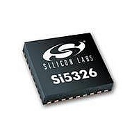
SI5326A-C-GM Silicon Laboratories Inc, SI5326A-C-GM Datasheet - Page 19

SI5326A-C-GM
Manufacturer Part Number
SI5326A-C-GM
Description
IC ANY-RATE MULTI/ATTEN 36-QFN
Manufacturer
Silicon Laboratories Inc
Type
Clock Multiplierr
Datasheet
1.SI5326B-C-GM.pdf
(72 pages)
Specifications of SI5326A-C-GM
Package / Case
36-QFN
Pll
Yes
Input
Clock
Output
CML, CMOS, LVDS, LVPECL
Number Of Circuits
1
Ratio - Input:output
2:2
Differential - Input:output
Yes/Yes
Frequency - Max
1.4GHz
Divider/multiplier
Yes/Yes
Voltage - Supply
1.71 V ~ 3.63 V
Operating Temperature
-40°C ~ 85°C
Mounting Type
Surface Mount
Frequency-max
1.4GHz
Max Input Freq
710 MHz
Max Output Freq
945 MHz
Maximum Operating Temperature
+ 85 C
Minimum Operating Temperature
- 40 C
Mounting Style
SMD/SMT
Number Of Outputs
2
Supply Current
251 mA
Supply Voltage (max)
3.3 V
Supply Voltage (min)
1.8 V
Lead Free Status / RoHS Status
Lead free / RoHS Compliant
Lead Free Status / RoHS Status
Lead free / RoHS Compliant, Lead free / RoHS Compliant
Available stocks
Company
Part Number
Manufacturer
Quantity
Price
Part Number:
SI5326A-C-GMR
Manufacturer:
SILICON LABS/èٹ¯ç§‘
Quantity:
20 000
The Si5326 has two differential clock outputs. The
electrical format of each clock output is independently
programmable to support LVPECL, LVDS, CML, or
CMOS loads. If not required, the second clock output
can be powered down to minimize power consumption.
The phase difference between the selected input clock
and the output clocks is adjustable in 200 ps increments
for system skew control using the CLAT[7:0] register.
Fine phase adjustment is available and is set using the
FLAT register bits. The nominal range and resolution of
the FLAT[14:0] skew adjustment word are: ±110 ps and
3 ps, respectively. In addition, the phase of one output
clock may be adjusted in relation to the phase of the
other output clock. The resolution varies from 800 ps to
2.2 ns depending on the PLL divider settings. See
Table 8 for instructions on ensuring output-to-output
alignment. The input to output skew is not specified.
The DSPLLsim software utility determines the phase
offset
multiplication
debugging, a bypass mode is available which drives the
output clock directly from the input clock, bypassing the
internal DSPLL. The device is powered by a single 1.8,
2.5, or 3.3 V supply.
resolution
CKOUT_ALWAYS_ON
ratio
for
combination.
0
0
1
1
Table 8. CKOUT_ALWAYS_ON and SQ_ICAL Truth Table
a
given
input
For
SQ_ICAL
system-level
clock/clock
0
1
0
1
Rev. 1.0
CKOUT OFF until after the first ICAL
CKOUT OFF until after the first successful
ICAL (i.e., when LOL is low)
CKOUT always ON, including during an ICAL
CKOUT always ON, including during an ICAL.
Use these settings to preserve output-to-output
skew
4.1. External Reference
An
114.285 MHz 3rd overtone crystal is used as part of a
fixed-frequency oscillator within the DSPLL. This
external reference is required for the device to perform
jitter attenuation. Silicon Laboratories recommends
using a high quality crystal. Specific recommendations
may be found in the Family Reference Manual.
In digital hold, the DSPLL remains locked and tracks the
external reference. Note that crystals can have
temperature sensitivities.
4.2. Further Documentation
Consult the Silicon Laboratories Si53xx Any Frequency
Precision Clock Family Reference Manual (FRM) for
detailed information about the Si5326 functions.
Additional design support is available from Silicon
Laboratories through your distributor.
Silicon Laboratories has developed a PC-based
software utility called DSPLLsim to simplify device
configuration, including frequency planning and loop
bandwidth selection. The FRM and this utility can be
downloaded from http://www.silabs.com/timing.
external,
high
Results
quality
clock
or
Si5326
a
low-cost
19


