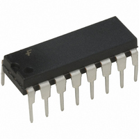
CD4046BCN Fairchild Semiconductor, CD4046BCN Datasheet - Page 12

CD4046BCN
Manufacturer Part Number
CD4046BCN
Description
IC LOCK LOOP CMOS PHASE 16-DIP
Manufacturer
Fairchild Semiconductor
Type
Phase Lock Loop (PLL)r
Datasheet
1.CD4046BCN.pdf
(14 pages)
Specifications of CD4046BCN
Pll
No
Input
Clock
Output
Clock
Number Of Circuits
1
Ratio - Input:output
1:2
Differential - Input:output
No/No
Frequency - Max
1.6MHz
Divider/multiplier
No/No
Voltage - Supply
3 V ~ 15 V
Operating Temperature
-55°C ~ 125°C
Mounting Type
Through Hole
Package / Case
16-DIP (0.300", 7.62mm)
Frequency-max
1.3MHz
Lead Free Status / RoHS Status
Lead free / RoHS Compliant
Other names
4046
4046B
CD4046
4046B
CD4046
www.fairchildsemi.com
VCO Component
Selection
Design Information
References
G.S. Moschytz, “Miniaturized RC Filters Using Phase-Locked Loop”, BSTJ, May, 1965.
Floyd Gardner, “Phaselock Techniques”, John Wiley & Sons, 1966.
Characteristics
Given: f
Use f
Figure 5 to
determine R1 and C1.
VCO Without Offset
o
with
o
R2
.
(Continued)
Using Phase Comparator I
Given: f
Calculate f
from the equation
f
Use f
determine R2 and C1.
Calculate
from the equation
Use
to determine ratio R2/
R1 to obtain R1.
min
with Figure 7
VCO With Offset
min
f
o
o
with Figure 6 to
and f
f
min
L
12
.
L
.
Given: f
Calculate f
the equation
Use f
determine R1 and C1. Use
VCO Without Offset
o
with Figure 5 to
max
R2
Using Phase Comparator II
o
.
from
Given: f
Use f
Figure 6 to
to determine R2 and
C1.
Calculate
to determine ratio
R2/R1 to obtain R1.
with Figure 7
VCO With Offset
min
min
with
and f
max
.


