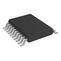
ADF4218LBRU-REEL7 Analog Devices Inc, ADF4218LBRU-REEL7 Datasheet

ADF4218LBRU-REEL7
Specifications of ADF4218LBRU-REEL7
Related parts for ADF4218LBRU-REEL7
ADF4218LBRU-REEL7 Summary of contents
Page 1
FEATURES Total Bandwidth/RF 3.0 GHz ADF4217L/ADF4218L, IF 1.1 GHz ADF4219L, IF 1.0 GHz 2 3.3 V Power Supply 1.8 V Logic Compatibility Separate V Allows Extended Tuning Voltage P Selectable Dual Modulus ...
Page 2
ADF4217L/ADF4218L/ADF4219L–SPECIFICATIONS ( 2 3 Parameter RF CHARACTERISTICS RF Input Frequency ( ADF4217L, ADF4218L ADF4217L, ADF4218L ADF4219L RF Input Sensitivity ...
Page 3
Parameter 6 NOISE CHARACTERISTICS 7 RF Phase Noise Floor 7 IF Phase Noise Floor 8 Phase Noise Performance Spurious Signals NOTES 1 Operating temperature ...
Page 4
ADF4217L/ADF4218L/ADF4219L 1, 2 ABSOLUTE MAXIMUM RATINGS ( T = 25°C, unless otherwise noted GND . . . . . . . . . . . . . . . . . . . . . ...
Page 5
TSSOP DGND 4 RF ADF4217L ADF4218L AGND 7 RF REF 8 IN DGND 9 IF MUXOUT 10 CHIP SCALE 24 23 ...
Page 6
ADF4217L/ADF4218L/ADF4219L Mnemonic Function V 1 Positive Power Supply for the RF Section. Decoupling capacitors to the analog ground plane should be placed as DD close as possible to this pin. V potential Power Supply ...
Page 7
Typical Performance Characteristics– 0 –5 –10 –15 –20 – –30 –35 –40 0 0.5 1.0 1.5 2.0 RF INPUT FREQUENCY – GHz TPC 1. Input Sensitivity, RF Input 0 –5 –10 –15 –20 –25 –30 –35 –40 0.1 ...
Page 8
ADF4217L/ADF4218L/ADF4219L 3V, V REFERENCE DD –10 LEVEL = –4.2dBm I = 4.0mA CP PFD FREQUENCY = 200kHz –20 LOOP BANDWIDTH = 20kHz RES. BANDWIDTH = 10kHz –30 VIDEO BANDWIDTH = 10kHz SWEEP = 1.9 SECONDS –40 AVERAGES ...
Page 9
CIRCUIT DESCRIPTION Reference Input Section The reference input stage is shown in Figure 2. SW1 and SW2 are normally closed switches; SW3 is normally open. When power-down is initiated, SW3 is closed and SW1 and SW2 are opened. This ensures ...
Page 10
ADF4217L/ADF4218L/ADF4219L The A and B counters, in conjunction with the dual modulus prescaler, make it possible to generate output frequencies that are spaced only by the Reference Frequency divided by R. The equation for the VCO frequency is as follows: ...
Page 11
Table II. ADF4217L/ADF4218L Family Latch Summary DB21 DB20 DB19 DB18 DB17 DB16 DB21 DB20 DB19 DB18 DB17 DB16 P7 P6 B11 B10 B9 B8 DB21 DB20 DB19 DB18 DB17 DB16 P12 P11 P10 P13 P9 ...
Page 12
ADF4217L/ADF4218L/ADF4219L DB21 DB20 DB19 DB18 DB17 DB16 R15 DB21 DB20 DB19 DB18 DB17 DB16 P7 P6 B13 B12 B11 B10 DB21 DB20 DB19 DB18 DB17 DB16 P13 P12 P11 P10 P9 R15 DB21 DB20 DB19 ...
Page 13
Table IV. ADF4217L/ADF4218L/ADF4219L IF Reference Counter Latch Map DB21 DB20 DB19 DB18 DB17 DB16 R15 P1 PD POLARITY 0 NEGATIVE 1 POSITIVE 1.0mA 1 4.0mA CHARGE PUMP P2 OUTPUT 0 NORMAL ...
Page 14
ADF4217L/ADF4218L/ADF4219L Table V. ADF4217L/ADF4218L IF AB Counter Latch Map DB21 DB20 DB19 DB18 DB17 DB16 P7 P6 B11 B10 B9 B8 B11 B10 ...
Page 15
DB21 DB20 DB19 DB18 DB17 DB16 P7 P6 B13 B12 B11 B10 B13 B12 B11 ...
Page 16
ADF4217L/ADF4218L/ADF4219L DB21 DB20 DB19 DB18 DB17 DB16 P12 P11 P10 P13 P9 R15 P9 PD POLARITY 0 NEGATIVE 1 POSITIVE I P13 CP 0 1.0mA 1 4.0mA CHARGE PUMP P10 OUTPUT 0 NORMAL 1 THREE-STATE P4 P12 P11 FROM RF ...
Page 17
Table VIII. ADF4217L/ADF4218L RF AB Counter Latch Map DB21 DB20 DB19 DB18 DB17 DB16 P16 P14 B11 B10 B9 B8 B11 B10 ...
Page 18
ADF4217L/ADF4218L/ADF4219L DB21 DB20 DB19 DB18 DB17 DB16 P16 P14 B13 B12 B11 B10 B13 B12 B11 ...
Page 19
PROGRAM MODES Tables IV and VII show how to set up the program modes in the ADF4217L family. The following should be noted and RF Analog Lock Detect indicate when the PLL is in lock. When the loop ...
Page 20
ADF4217L/ADF4218L/ADF4219L RF Program Modes Tables IV and VII show how to set up the RF program modes. RF Charge Pump Currents P13 sets the RF charge pump current. With P13 set to “0,” I 1.0 mA. With P13 set to ...
Page 21
IF OUT 100pF 18 100pF VCO190-200T 18 450pF 100pF 51 10MHz TCXO DECOUPLING CAPACITORS (22 F/10pF THE TCXO AND THE VCOs HAVE BEEN OMITTED FROM THE DIAGRAM TO AID CLARITY. CC Figure ...
Page 22
ADF4217L/ADF4218L/ADF4219L 20-Lead Thin Shrink Small Outline Package [TSSOP] PIN 1 0.15 0.05 COPLANARITY 0.10 4.50 BSC TOP VIEW PIN 1 INDEX AREA 1 24 BOTTOM VIEW OUTLINE DIMENSIONS (RU-20) Dimensions shown in millimeters 6.60 6.50 6. 4.50 4.40 ...
Page 23
Revision History Location 5/03—Data Sheet changed from REV REV. C. Change to SPECIFICATIONS . . . . . . . . . . . . . . . . . . . . . . . . . ...
Page 24
–24– ...


