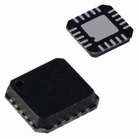
ADF4154BCP Analog Devices Inc, ADF4154BCP Datasheet - Page 6

ADF4154BCP
Manufacturer Part Number
ADF4154BCP
Description
IC FRACTION-N FREQ SYNTH 20LFCSP
Manufacturer
Analog Devices Inc
Type
Fractional N Synthesizer (RF)r
Datasheet
1.ADF4154BRUZ.pdf
(24 pages)
Specifications of ADF4154BCP
Pll
Yes
Input
CMOS
Output
Clock
Number Of Circuits
1
Ratio - Input:output
2:1
Differential - Input:output
Yes/No
Frequency - Max
4GHz
Divider/multiplier
No/Yes
Voltage - Supply
2.7 V ~ 3.3 V
Operating Temperature
-40°C ~ 85°C
Mounting Type
Surface Mount
Package / Case
20-LFCSP
Frequency-max
4GHz
For Use With
EVAL-ADF4154EBZ1 - BOARD EVALUATION FOR ADF4154EB1
Lead Free Status / RoHS Status
Contains lead / RoHS non-compliant
ADF4154
PIN CONFIGURATION AND PIN FUNCTION DESCRIPTIONS
Table 4. Pin Function Descriptions
TSSOP
1
2
3
4
5
6
7
8
9
10
11
12
13
14
15
16
LFCSP
19
20
1
2, 3
4
5
6, 7
8
9, 10
11
12
13
14
15
16, 17
18
CPGND
AGND
RF
RF
REF
AV
R
Figure 3. TSSOP Pin Configuration
SET
IN
IN
CP
DD
IN
B
A
Mnemonic
R
CP
CPGND
AGND
RF
RF
AV
REF
DGND
SDV
CLK
DATA
LE
MUXOUT
DV
V
1
2
3
4
5
6
7
8
SET
P
IN
IN
DD
DD
(Not to Scale)
IN
B
A
ADF4154
DD
TOP VIEW
Description
Set Resistor. Connecting a resistor between this pin and ground sets the maximum charge pump
output current. The relationship between I
where R
Charge Pump Output. When enabled, this pin provides ±I
drives the external VCO.
Charge Pump Ground. This is the ground return path for the charge pump.
Analog Ground. This is the ground return path of the prescaler.
Complementary Input to the RF Prescaler. This point should be decoupled to the ground plane with a
small bypass capacitor, typically 100 pF (see Figure 15).
Input to the RF Prescaler. This small-signal input is normally ac-coupled from the VCO.
Positive Power Supply for the RF Section. Decoupling capacitors to the digital ground plane should be placed
as close as possible to this pin. AV
Reference Input. This CMOS input has a nominal threshold of V
100 kΩ (see Figure 14). This input can be driven from a TTL or CMOS crystal oscillator, or it can be ac-coupled.
Digital Ground.
Σ-∆ Power. Decoupling capacitors to the digital ground plane should be placed as close as possible to
this pin. SDV
Serial Clock Input. This serial clock is used to clock in the serial data to the registers. The data is latched
into the shift register on the CLK rising edge. This input is a high impedance CMOS input.
Serial Data Input. The serial data is loaded MSB first with the two LSBs as the control bits. This input is a
high impedance CMOS input.
Load Enable, CMOS Input. When LE is high, the data stored in the shift registers is loaded into one of the
four latches, which is selected by the user via the control bits.
Multiplexer Output. This pin allows either the RF lock detect, the scaled RF, or the scaled reference
frequency to be accessed externally.
Positive Power Supply for the Digital Section. Decoupling capacitors to the digital ground plane should
be placed as close as possible to this pin. DV
voltage as AV
Charge Pump Power Supply. This should be greater than or equal to V
can be set to 5.5 V and used to drive a VCO with a tuning range of up to 5.5 V.
16
15
14
13
12
11
10
9
V
DV
MUXOUT
LE
DATA
CLK
SDV
DGND
P
I
DD
CPmax
DD
SET
= 5.1 kΩ and I
=
DD
DD
25
R
has a value of 3 V ± 10%. SDV
SET
.
5 .
CPmax
Rev. A | Page 6 of 24
= 5 mA.
DD
has a value of 3 V ± 10%. AV
CP
DD
DD
and R
has a value of 3 V ± 10%. DV
must have the same voltage as DV
SET
is
CPGND
AGND
AGND
RF
RF
IN
IN
Figure 4. LFCSP Pin Configuration
CP
B
A
to the external loop filter, which in turn
1
2
3
4
5
DD
/2 and an equivalent input resistance of
DD
(Not to Scale)
ADF4154
TOP VIEW
must have the same voltage as DV
PIN 1
INDICATOR
DD
. In systems where V
DD
must have the same
15
14
13
12
11
MUXOUT
LE
DATA
CLK
SDV
DD
DD
.
DD
is 3 V, it
DD
.


