CY24206ZXC-4 Cypress Semiconductor Corp, CY24206ZXC-4 Datasheet - Page 3
CY24206ZXC-4
Manufacturer Part Number
CY24206ZXC-4
Description
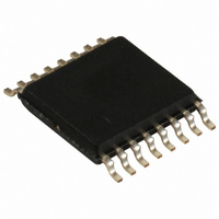
IC CLOCK GEN STB 3.3V 16-TSSOP
Manufacturer
Cypress Semiconductor Corp
Type
Clock Generator, Fanout Distributionr
Series
MediaClock™r
Datasheet
1.CY24206ZXC-4.pdf
(6 pages)
Specifications of CY24206ZXC-4
Number Of Circuits
1
Package / Case
16-TSSOP
Pll
Yes
Input
Clock
Output
Clock
Ratio - Input:output
1:4
Differential - Input:output
No/No
Frequency - Max
74.25MHz
Divider/multiplier
Yes/No
Voltage - Supply
3.135 V ~ 3.465 V
Operating Temperature
0°C ~ 70°C
Mounting Type
Surface Mount
Frequency-max
74MHz
Minimum Input Frequency
27 MHz
Output Frequency Range
24.725 MHz to 81.081 MHz
Supply Voltage (max)
3.465 V
Supply Voltage (min)
3.135 V
Maximum Operating Temperature
+ 70 C
Minimum Operating Temperature
0 C
Mounting Style
SMD/SMT
Operating Supply Voltage
3.3 V
Lead Free Status / RoHS Status
Lead free / RoHS Compliant
Available stocks
Company
Part Number
Manufacturer
Quantity
Price
Company:

Part Number:
CY24206ZXC-4T
Manufacturer:
CY
Quantity:
3 870


Document #: 38-07451 Rev. *B
Absolute Maximum Conditions
Recommended Operating Conditions
DC Electrical Specifications
AC Electrical Specifications
Test and Measurement Set-up
Note:
V
V
T
V
T
C
f
I
I
I
I
V
V
I
I
R
DC
ER
EF
t
t
1. Not 100% tested.
REF
Parameter
OH
OL
IH
IL
VDD
VDDL
9
10
Parameter
J
A
DD
DDL
DD
IH
IL
LOAD
UP
Parameter
Parameter
/AV
DDL
/V
[1]
[1]
DDL
Output High Current
Output Low Current
Input High Current
Input Low Current
Input High Voltage
Input Low Voltage
Supply Current
Supply Current
Pull-up resistor on Inputs
Output Duty Cycle
Rising Edge Rate
Falling Edge Rate
Clock Jitter
PLL Lock Time
Supply Voltage
I/O Supply Voltage
Junction Temperature
Digital Inputs
Electrostatic Discharge
Operating Voltage
Ambient Temperature
Max. Load Capacitance
Reference Frequency
Name
Name
V
Description
Description
DDs
0.1 µF
Duty Cycle is defined in Figure 1; t1/t2, 50% of
V
Output Clock Edge Rate, Measured from 20% to
80% of V
Output Clock Edge Rate, Measured from 80% to
20% of V
CLK1, CLK2 Peak-Peak period jitter
DD
V
V
V
V
CMOS levels, 70% of V
CMOS levels, 30% of V
AV
V
V
OH
OL
IH
IL
DDL
DD
DD
= 0V
= V
= 0.5, V
= V
= 3.14 to 3.47V, measured V
/V
Current
DD
DD
DD
DD
DD
, C
, C
GND
Current
– 0.5, V
LOAD
LOAD
DD
/V
Description
Description
DUT
DDL
= 15 pF. See Figure 2.
= 15 pF. See Figure 2.
3.135
Min.
DD
AV
0
= 3.3V
/V
SS
Min.
–0.5
DD
DD
DDL
2
– 0.3
= 3.3V
IN
= 0V
Typ.
3.3
27
C
LOAD
Outputs
AV
Min.
Min.
0.7
12
12
0.8
0.8
45
–
–
DD
Max.
125
7.0
7.0
+ 0.3
3.465
Max.
Typ.
Typ.
100
200
1.4
1.4
24
24
50
70
15
5
–
Max.
Max.
CY24206
150
55
0.3
10
50
25
20
3
Page 3 of 6
Unit
MHz
Unit
°C
kV
°C
pF
V
V
V
V
V/ns
V/ns
Unit
VDD
VDD
Unit
ms
mA
mA
mA
mA
ps
kΩ
%
µA
µA
[+] Feedback
Related parts for CY24206ZXC-4
Image
Part Number
Description
Manufacturer
Datasheet
Request
R

Part Number:
Description:
Manufacturer:
Cypress Semiconductor Corp
Datasheet:
Part Number:
Description:
Manufacturer:
Cypress Semiconductor Corp
Datasheet:
Part Number:
Description:
Manufacturer:
Cypress Semiconductor Corp
Datasheet:
Part Number:
Description:
Manufacturer:
Cypress Semiconductor Corp
Datasheet:
Part Number:
Description:
Manufacturer:
Cypress Semiconductor Corp
Datasheet: