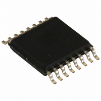
CY25200FZXC Cypress Semiconductor Corp, CY25200FZXC Datasheet

CY25200FZXC
Specifications of CY25200FZXC
Available stocks
Related parts for CY25200FZXC
CY25200FZXC Summary of contents
Page 1
... OSC. XOUT XOUT XIN Cypress Semiconductor Corporation Document #: 38-07633 Rev. *F Programmable Spread Spectrum Clock Generator for EMI Reduction Description The CY25200 is a programmable clock generator with spread spectrum capability. Spread spectrum modulates the output clock frequency over a small range, spreading the energy and reducing the energy peak ...
Page 2
Pin Configuration General Description The CY25200 is a Spread Spectrum Clock Generator (SSCG) IC used to reduce Electro Magnetic Interference (EMI) found in today’s high speed digital electronic systems. The device uses a Cypress proprietary Phase-Locked Loop (PLL) and Spread ...
Page 3
Table 2. Fixed Function Pins Pin Function Output Clock Frequency Pin Name SSCLK[1:6] Pin 12, 14, 15 Units MHz Program Value USER SPECIFIED CLKSEL = 0 Program Value USER SPECIFIED CLKSEL = 1 Table 3. Multi-Function Pins ...
Page 4
Product Functions Control Pins (CP0, CP1, CP2 and CP3) Four control signals are available through programming of pins 4, 10, 14, and 15. CP0 (pin 4) and CP1 (pin10) are specifically designed to function as control pins. However, pins 14 ...
Page 5
Spread Percentage (SSCLK1 to SSCLK6 Outputs) The SSCLK frequency is programmed to a percentage value from ±0.25% to ±2.5% for center spread and from –0.5% to –5.0% down spread. The granularity is 0.25%. Table 4. Using Clock Select, CLKSEL Control ...
Page 6
Switching Waveforms Figure 5. Output Rise and Fall Time (SSCLK and REFCLK) OUTPUT Tr Output Rise time (Tr Output Fall time (Tf Refer to AC Electrical Characteristics table for SR (Slew Rate) ...
Page 7
Informational Graphs The informational graphs are meant to convey the typical performance levels. No performance specifications is implied or guaranteed. 172.5 171.5 Spread Spectrum Profile: Fnom=166MHz, Fmod=30kHz, Spread%= -4% 170.5 169.5 168.5 167.5 166.5 165.5 164.5 163.5 162.5 161.5 160.5 ...
Page 8
Absolute Maximum Rating Supply Voltage (VDD)....................................... –0.5 to +7.0V DC Input Voltage ......................................–0. Storage Temperature (non-condensing) ..... –55°C to +125°C Junction Temperature ................................ –40°C to +125°C Recommended Crystal Specifications Parameter Description F Nominal Crystal Frequency NOM C Nominal ...
Page 9
AC Electrical Specifications Parameter Description DC Output Duty Cycle Output Duty Cycle SR1 Rising/Falling Edge Slew Rate SSCLK1/2/3/4 < 100 MHz, V Rising/Falling Edge Slew Rate SSCLK1/2/3/4 ≥ 100 MHz, V SR2 SR3 Rising/Falling Edge Slew Rate SSCLK1/2/3/4 < 100 ...
Page 10
... Ordering Code [6] CY25200-ZXCxxxw 16-Pin TSSOP (Pb-free) [6] CY25200-ZXCxxxwT 16-Pin TSSOP – Tape and Reel (Pb-free) [6] CY25200FZXC 16-Pin TSSOP (Pb-free) CY25200K-ZXCxxxw 16-Pin TSSOP (Pb-free) CY25200K-ZXCxxxwT 16-Pin TSSOP – Tape and Reel (Pb-free) CY25200KFZXC 16-Pin TSSOP (Pb-free) CY25200KFZXCT 16-Pin TSSOP – Tape and Reel (Pb-free) ...
Page 11
... SKEW Removed specific PD# and OE pin nos. from parameters T Standardized timing parameter names to upper case Corrected part numbers in Ordering Information Table Removed part number CY25200FZXCT Added part number CY25200KFZXCT Replaced CY3672 and CY3672-PRG with CY3672-USB CY25200 for clarity values, ...
Page 12
... Cypress against all charges. Any Source Code (software and/or firmware) is owned by Cypress Semiconductor Corporation (Cypress) and is protected by and subject to worldwide patent protection (United States and foreign), United States copyright laws and international treaty provisions. Cypress hereby grants to licensee a personal, non-exclusive, non-transferable license to copy, use, modify, create derivative works of, and compile the Cypress Source Code and derivative works for the sole purpose of creating custom software and or firmware in support of licensee product to be used only in conjunction with a Cypress integrated circuit as specified in the applicable agreement ...


