CY28RS480ZXC Cypress Semiconductor Corp, CY28RS480ZXC Datasheet - Page 3
CY28RS480ZXC
Manufacturer Part Number
CY28RS480ZXC
Description
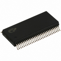
IC CLOCK GENERATOR 56-TSSOP
Manufacturer
Cypress Semiconductor Corp
Type
Clock Generatorr
Datasheet
1.CY28RS480OXC.pdf
(15 pages)
Specifications of CY28RS480ZXC
Frequency - Max
200MHz
Voltage - Supply
3.135 V ~ 3.465 V
Operating Temperature
0°C ~ 70°C
Mounting Type
Surface Mount
Package / Case
56-TSSOP II
Frequency-max
200MHz
Lead Free Status / RoHS Status
Lead free / RoHS Compliant
Output
-
Input
-
Available stocks
Company
Part Number
Manufacturer
Quantity
Price
Company:

Part Number:
CY28RS480ZXC
Manufacturer:
MAXIM
Quantity:
160
Part Number:
CY28RS480ZXC
Manufacturer:
CYPRESS/赛普拉斯
Quantity:
20 000


Document #: 38-07638 Rev. *C
Serial Data Interface
To enhance the flexibility and function of the clock synthesizer,
a two-signal serial interface is provided. Through the Serial
Data Interface, various device functions, such as individual
clock output buffers, can be individually enabled or disabled.
The registers associated with the Serial Data Interface
initializes to their default setting upon power-up, and therefore
use of this interface is optional. Clock device register changes
are normally made upon system initialization, if any are
required. The interface cannot be used during system
operation for power management functions.
Table 1. Command Code Definition
Table 2. Block Read and Block Write Protocol
Table 3. Byte Read and Byte Write Protocol
18:11
27:20
36:29
45:38
(6:5)
(4:0)
8:2
8:2
Bit
Bit
Bit
10
19
28
37
46
....
....
....
....
10
1
9
1
9
7
Start
Slave address – 7 bits
Write
Acknowledge from slave
Command Code – 8 bits
Acknowledge from slave
Byte Count – 8 bits
Acknowledge from slave
Data byte 1 – 8 bits
Acknowledge from slave
Data byte 2 – 8 bits
Acknowledge from slave
Data Byte /Slave Acknowledges
Data Byte N – 8 bits
Acknowledge from slave
Stop
Start
Slave address – 7 bits
Write
Acknowledge from slave
0 = Block read or block write operation, 1 = Byte read or byte write operation
Chip select address, set to ‘00’ to access device
Byte offset for byte read or byte write operation. For block read or block write operations, these bits should be '00000'
Block Write Protocol
Byte Write Protocol
Description
Description
Description
Data Protocol
The clock driver serial protocol accepts byte write, byte read,
block write, and block read operations from the controller. For
block write/read operation, the bytes must be accessed in
sequential order from lowest to highest byte (most significant
bit first) with the ability to stop after any complete byte has
been transferred. For byte write and byte read operations, the
system controller can access individually indexed bytes. The
offset of the indexed byte is encoded in the command code,
as described in Table 1.
The block write and block read protocol is outlined in Table 2
while Table 3 outlines the corresponding byte write and byte
read protocol. The slave receiver address is 11010010 (D2h).
27:21
37:30
46:39
55:48
18:11
Bit
8:2
10
19
20
28
29
38
47
56
....
....
....
8:2
Bit
10
1
9
1
9
Data byte 1 from slave – 8 bits
Start
Slave address – 7 bits
Write
Acknowledge from slave
Command Code – 8 bits
Acknowledge from slave
Repeat start
Slave address – 7 bits
Read = 1
Acknowledge from slave
Byte Count from slave – 8 bits
Acknowledge
Acknowledge
Data byte 2 from slave – 8 bits
Acknowledge
Data bytes from slave / Acknowledge
Data Byte N from slave – 8 bits
NOT Acknowledge
Start
Slave address – 7 bits
Write
Acknowledge from slave
Block Read Protocol
Byte Read Protocol
Description
Description
CY28RS480
Page 3 of 15
[+] Feedback
Related parts for CY28RS480ZXC
Image
Part Number
Description
Manufacturer
Datasheet
Request
R

Part Number:
Description:
Manufacturer:
Cypress Semiconductor Corp
Datasheet:
Part Number:
Description:
Manufacturer:
Cypress Semiconductor Corp
Datasheet:
Part Number:
Description:
Manufacturer:
Cypress Semiconductor Corp
Datasheet:
Part Number:
Description:
Manufacturer:
Cypress Semiconductor Corp
Datasheet:
Part Number:
Description:
Manufacturer:
Cypress Semiconductor Corp
Datasheet: