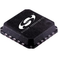
SI5310-BM Silicon Laboratories Inc, SI5310-BM Datasheet - Page 23

SI5310-BM
Manufacturer Part Number
SI5310-BM
Description
IC CLOCK MULTIPLIER/REGEN 20MLP
Manufacturer
Silicon Laboratories Inc
Type
Clock Multiplierr
Datasheet
1.SI5310-BM.pdf
(26 pages)
Specifications of SI5310-BM
Package / Case
20-VQFN Exposed Pad, 20-HVQFN, 20-SQFN, 20-DHVQFN
Pll
Yes with Bypass
Input
Clock
Output
CML
Number Of Circuits
1
Ratio - Input:output
1:2
Differential - Input:output
Yes/Yes
Frequency - Max
668MHz
Divider/multiplier
Yes/Yes
Voltage - Supply
2.375 V ~ 2.625 V
Operating Temperature
-40°C ~ 85°C
Mounting Type
Surface Mount
Frequency-max
668MHz
Mounting Style
SMD/SMT
Description/function
Multiplier/Regenratr 155MHz 622MHz
Lead Free Status / RoHS Status
Contains lead / RoHS non-compliant
Other names
336-1139
9. 4x4 mm 20L MLP Recommended PCB Layout
Notes:
1. All dimensions listed are in millimeters (mm).
2. The perimeter pads are to be Non-Solder Mask Defined (NSMD). Solder mask openings should be designed to leave 60-75 mm
3. The center thermal pad is to be Solder Mask Defined (SMD).
4. Thermal/Ground vias placed in the center pad should be no less than 0.2 mm (8 mil) diameter and tented from the top to prevent
5. The stencil aperture should match the pad size (1:1 ratio) for the perimeter pads. A 3x3 array of 0.5 mm square stencil openings, on a
6. A stencil thickness of 5 mil is recommended. The stencil should be laser cut and electropolished, with trapezoidal walls to facilitate
7. A “No-Clean”, Type 3 solder paste should be used for assembly. Nitrogen purge during reflow is recommended.
8. Do not place any signal or power plane vias in these “keep out” regions.
9. Suggest four 0.38 mm (15 mil) vias to the ground plane.
Symbol
separation between solder mask and pad metal, all the way around the pad.
solder from flowing into the via hole.
0.65 mm pitch, should be used for the center thermal pad.
paste release.
G
A
D
R
X
Y
e
Z
Pad Row/Column Width/Length
Thermal Pad Width/Height
Pad Pitch
Pad Row/Column Separation
Pad Radius
Pad Width
Pad Length
Pad Row/Column Extents
See Note 8
Gnd Pin
Parameter
See Note 9
Rev. 1.2
2.23
2.03
2.43
0.23
4.26
Min
—
—
—
Dimensions
0.50 BSC
0.12 REF
0.94 REF
Nom
2.25
2.08
2.46
0.25
4.28
Si5310
Max
2.28
2.13
2.48
0.28
4.31
—
—
—
23


