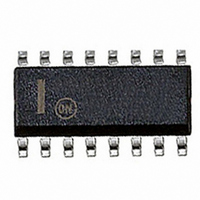
NB4N507ADR2 ON Semiconductor, NB4N507ADR2 Datasheet - Page 3

NB4N507ADR2
Manufacturer Part Number
NB4N507ADR2
Description
IC SYNTHESIZER CLK PECL 16-SOIC
Manufacturer
ON Semiconductor
Type
Clock/Frequency Synthesizerr
Datasheet
1.NB4N507ADR2G.pdf
(8 pages)
Specifications of NB4N507ADR2
Pll
Yes
Input
Clock, Crystal
Output
PECL
Number Of Circuits
1
Ratio - Input:output
1:1
Differential - Input:output
No/Yes
Frequency - Max
200MHz
Divider/multiplier
Yes/Yes
Voltage - Supply
3 V ~ 5.5 V
Operating Temperature
-40°C ~ 85°C
Mounting Type
Surface Mount
Package / Case
16-SOIC (3.9mm Width)
Frequency-max
200MHz
Lead Free Status / RoHS Status
Contains lead / RoHS non-compliant
Available stocks
Company
Part Number
Manufacturer
Quantity
Price
Part Number:
NB4N507ADR2G
Manufacturer:
ON/安森美
Quantity:
20 000
*The PECL Outputs are 15 mA open collector and must be DC loaded and AC terminated. See Figures 4, 5 and 6.
Stresses exceeding Maximum Ratings may damage the device. Maximum Ratings are stress ratings only. Functional operation above the
Recommended Operating Conditions is not implied. Extended exposure to stresses above the Recommended Operating Conditions may affect
device reliability.
2. JEDEC standard multilayer board - 2S2P (2 signal, 2 power).
Table 3. PIN DESCRIPTION
7,10,11,12,
Table 5. MAXIMUM RATINGS
Symbol
V
V
T
T
q
q
T
SOIC-16
A
stg
JA
JC
sol
CC
I
Pin #
2,3
5,6
15
13
14
16
1
4
8
9
Positive Power Supply
Input Voltage
Operating Temperature Range
Storage Temperature Range
Thermal Resistance (Junction-to-Ambient)
Thermal Resistance (Junction-to-Case)
Wave Solder
CLKOUT
CLKOUT
X1/CLK
Name
GND
V
NC
OE
S1
S0
X2
DD
Table 4. ATTRIBUTES
1. For additional information, see Application Note AND8003/D.
ESD Protection
Moisture Sensitivity, Indefinite Time Out of Drypack (Note 1)
Flammability Rating
Transistor Count
Meets or exceeds JEDEC Spec EIA/JESD78 IC Latchup Test
Parameter
(LV)CMOS/(LV)TTL
Tri-Level Input
Tri-Level Input
PECL Output*
PECL Output*
Power Supply
Power Supply
Crystal Input
Crystal Input
No Connect
Input
I/O
Characteristics
Pb-Free
Pb
Crystal or Clock Input
Positive Supply Voltage (3.0 V to 5.5 V)
Multiplier Select Pin; When Left Open, Defaults to V
Negative Supply Voltage
Pin 10 does not require an external resistor. The NB4N507A will function with or
without a resistor on Pin 10.
Non-inverted differential PECL clock output.
Inverted differential PECL clock output.
Output Enable for the CLKOUT/CLKOUT Outputs. Outputs are
enabled when HIGH or when left open; OE pin has internal pullup resistor. Disables
both outputs when LOW. CLKOUT goes LOW, CLKOUT goes HIGH.
Multiplier Select Pin; When Left Open, Defaults to V
Crystal Input
http://onsemi.com
< 3 sec @ 248°C
< 3 sec @ 260°C
Condition 1
GND = 0 V
NB4N507A
500 lfpm
Oxygen Index: 28 to 34
(Note 2)
Charged Device Model
0 lfpm
Human Body Model
3
Machine Model
Condition 2
SOIC-16
SOIC-16
Description
UL 94 V-0 @ 0.125 in
1145 Devices
> 150 V
GND - 0.5 ≤ V
Level 1
> 1 kV
> 1 kV
Value
DD
DD
-65 to +150
-40 to +85
B 2
B 2
33 to 36
Rating
100
265
265
60
6
I
≤ V
DD
+ 0.5
°C/W
°C/W
°C/W
Unit
°C
°C
°C
V
V


