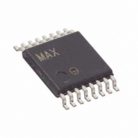
DS1123LE-50+ Maxim Integrated Products, DS1123LE-50+ Datasheet - Page 6

DS1123LE-50+
Manufacturer Part Number
DS1123LE-50+
Description
IC TIMING ELEMENT PROG 16-TSSOP
Manufacturer
Maxim Integrated Products
Datasheet
1.DS1123LE-200.pdf
(14 pages)
Specifications of DS1123LE-50+
Number Of Taps/steps
256
Function
Programmable
Delay To 1st Tap
16.5nS
Tap Increment
0.5nS
Available Total Delays
127.5ns
Voltage - Supply
3 V ~ 3.6 V
Operating Temperature
0°C ~ 70°C
Mounting Type
Surface Mount
Package / Case
16-TSSOP
Lead Free Status / RoHS Status
Lead free / RoHS Compliant
Number Of Independent Delays
-
3.3V, 8-Bit, Programmable Timing Element
AC ELECTRICAL CHARACTERISTICS (DS1123L-100)
(V
Note 1:
Note 2:
Note 3:
Note 4:
Note 5:
Note 6:
Note 7:
Note 8:
Note 9:
6
Reference Delay
Delay Step Size
Step-Zero Delay with Respect
to IN
Step-Zero Delay with Respect
to REF
Maximum Delay with Respect
to IN
Delay with Respect to REF
Delay with Respect to REF
Tolerance
Voltage Delay Variation
Temperature Delay Variation
Integral Nonlinearity (Deviation
from Straight Line)
OUT Delta Delay
IN High to PWM High
Minimum PWM Output Pulse
Width
Minimum Input Pulse Width
Minimum Input Period
Input Rise and Fall Times
CC
______________________________________________________________________
= +3.0V to 3.6V, T
PARAMETER
All voltages are referenced to ground.
If IN is high during power-up, the output remains low until IN is toggled low and back high again.
The reference delay is closely matched to the step-zero delay to allow relative timings down to zero or less.
Measured from rising edge of the input to the rising edge of the output (t
Delay from input to output with a programmed delay value of zero.
This is the relative delay between REF and OUT. The device is designed such that when programmed to zero delay the
OUT output always appears before the REF output. This parameter is numerically equal to t
From rising edge to rising edge.
This is the actual measured delay from IN to OUT. This parameter exhibits greater temperature variation than the relative
delay parameter.
This is the actual measured delay with respect to the REF output. This parameter more closely reflects the programmed
delay value than the absolute delay parameter (see Figure 8). Typical delay shift due to aging is within ±0.85%. Aging
stressing includes level 1 moisture reflow preconditioning (24hr +125°C bake, 168hr +85°C/85%RH moisture soak, and
three solder reflow passes +260°C +0°C/-5°C peak) followed by 1000hr (max) V
ased +150°C bake, and 1000 temperature cycles at -55°C to +125°C.
A
= 0°C to +70°C.)
SYMBOL
t
Δt
t
t
t
t
D0REF
t
t
t
Δt
t
DMAX
DREF
Δt
t
PWM0
DREF
DREF
t
DREF
STEP
PWM
INV0
t
REF
t
DREF
t
t
r
D0
err
WI
DV
, t
DT
f
(Notes 3, 4)
T
(Notes 4, 5)
(Notes 6, 7)
(Notes 4, 8)
Position FF (Notes 7, 9)
V
(Notes 7, 9)
(Notes 7, 9)
V
(Note 10)
(Note 11)
(Notes 4, 12)
(Note 13)
(Note 14)
(Note 15)
(Note 16)
A
CC
CC
= +25°C
= 3.3V, T
= 3.3V (Notes 7, 9)
A
CONDITIONS
= +25°C
DR
).
CC
biased +125°C OP/L, 1000hr unbi-
-0.75
MIN
-2.5
-0.5
-2.5
40
80
-4
0
0
5
0
D0
- t
TYP
16.5
16.5
-1.5
272
255
18
REF
1
0
1
(see Figure 8).
+0.75
MAX
+0.5
+2.5
2.25
2.5
+4
22
22
22
0
1
UNITS
ns
ns
ns
ns
ns
ns
ns
ns
ns
ns
ns
ns
µs
%
%
%


