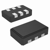
CY2XF32FLXCT Cypress Semiconductor Corp, CY2XF32FLXCT Datasheet - Page 4

CY2XF32FLXCT
Manufacturer Part Number
CY2XF32FLXCT
Description
IC XTAL OSC CMOS 6CLCC
Manufacturer
Cypress Semiconductor Corp
Datasheet
1.CY2XF32FLXCT.pdf
(9 pages)
Specifications of CY2XF32FLXCT
Pll
Yes
Input
Crystal
Output
CMOS
Number Of Circuits
1
Ratio - Input:output
1:1
Differential - Input:output
No/No
Frequency - Max
200MHz
Divider/multiplier
Yes/No
Voltage - Supply
*
Operating Temperature
*
Mounting Type
Surface Mount
Package / Case
6-CLCC
Frequency
*
Count
*
Operating Supply Voltage (typ)
2.5/3.3
Output Level
CMOS
Symmetry Max
55%
Operating Temp Range
0C to 70C
Screening Level
Commercial
Load Capacitance
15pF
Lead Free Status / RoHS Status
Lead free / RoHS Compliant
Absolute Maximum Conditions
Operating Conditions
DC Electrical Characteristics
Document Number: 001-53147 Rev. *C
V
V
T
T
ESD
Θ
V
T
T
C
I
I
V
V
I
V
V
I
I
I
I
C
C
Notes
Parameter
Parameter
Parameter
DD
SB
OZ
IH0
IH1
IL0
IL1
1. The voltage on any input or I/O pin cannot exceed the power pin during power up.
2. Simulated. The board is derived from the JEDEC multilayer standard. It measures 76 x 114 x 1.6 mm and has four layers of copper (2/1/1/2 oz.). The internal layers
3. Not 100% tested, guaranteed by design and characterization.
A
DD
IN
S
J
DD
PU
OH
OL
IH
IL
JA
LOAD
IN0
IN1
[1]
[2]
are 100% copper planes, while the top and bottom layers have 50% metalization. No vias are included in the model.
[3]
[3]
HBM
3.3V Supply Voltage Range
2.5V Supply Voltage Range
Power Up Time for V
is Monotonic)
Ambient Temperature, Commercial
Ambient Temperature, Industrial
Load Capacitance at CLK (>100 MHz)
Load Capacitance at CLK (≤100 MHz)
Operating Supply Current
Standby Supply Current
Output High Voltage
Output Low Voltage
Output Leakage Current
Input High Voltage
Input Low Voltage
Input High Current, OE/PD# Pin
Input High Current, FS0 & FS1 Pins Input = V
Input Low Current, OE/PD# Pin
Input Low Current, FS0 & FS1 Pin
Input Capacitance, OE/PD# Pin
Input Capacitance, FS0 & FS1 Pin
Supply Voltage
Input Voltage, DC
Temperature, Storage
Temperature, Junction
ESD Protection (Human Body Model)
Thermal Resistance, Junction to Ambient
Description
Description
DD
to Reach Minimum Specified Voltage (Power Ramp
Description
PRELIMINARY
V
unloaded
PD# = V
V
V
OE/PD# = V
Input = V
Input = V
Input = V
DD
DD
DD
= 3.465V, OE/PD# = V
= min, I
= max, I
Relative to V
Non operating
JEDEC STD 22-A114-B
0 m/s airflow
SS
DD
DD
SS
SS
OH
SS
OL
Condition
= –4 mA
= 4 mA
Condition
SS
DD
, output
0.9*V
0.7*V
3.135
2.375
0.05
Min
Min
–35
–50
–20
–40
2000
–0.5
–0.5
Min
–55
–40
0
–
–
–
–
–
–
–
–
–
–
DD
DD
Typ
64
Typ
3.3
2.5
15
–
–
–
–
–
–
–
–
–
–
–
4
–
–
–
–
–
V
DD
Max
135
135
4.4
0.1*V
0.3*V
–
+0.5
3.465
2.625
Max
500
Max
200
110
115
70
85
10
15
35
10
–
–
–
–
–
–
CY2XF32
DD
DD
Page 4 of 9
°C/W
Unit
Unit
Unit
°C
°C
ms
°C
°C
pF
pF
mA
V
V
V
V
V
μA
μA
μA
μA
μA
μA
pF
pF
V
V
V
V
[+] Feedback


