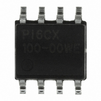
PI6CX100-00WE Pericom Semiconductor, PI6CX100-00WE Datasheet - Page 2

PI6CX100-00WE
Manufacturer Part Number
PI6CX100-00WE
Description
IC VCXO 3.3V GEN-PURPOSE 8-SOIC
Manufacturer
Pericom Semiconductor
Type
Voltage Controlled Crystal Oscillator (VCXO)r
Datasheet
1.PI6CX100-00WE.pdf
(4 pages)
Specifications of PI6CX100-00WE
Frequency
40MHz
Voltage - Supply
3.135 V ~ 3.465 V
Current - Supply
5mA
Operating Temperature
-20°C ~ 70°C
Package / Case
8-SOIC
Output Level
CMOS
Frequency Stability
±30
Symmetry Max
55%
Operating Supply Voltage (typ)
3.3
Pin Count
8
Mounting Style
Surface Mount
Screening Level
Industrial
Frequency Tolerance
±20
Product Height (mm)
1.5mm
Product Depth (mm)
3.99mm
Product Length (mm)
5mm
Rad Hardened
No
Lead Free Status / RoHS Status
Lead free / RoHS Compliant
Count
-
Lead Free Status / RoHS Status
Lead free / RoHS Compliant, Compliant
Maximum Ratings
(Above which the useful life may be impaired. For user guidelines, not tested.)
DC Electrical Characteristics
(Unless otherwise specified, V
AC Electrical Characteristics
Storage Temperature .........................................–55°C to 125°C
Ambient Temperature ........................................–40°C to 85°C
Supply Voltage V
Inputs/Outputs Voltage.............................. –0.5V to V
Output Current ..................................................................10mA
Soldering Lead Temperature (10s)................................... 260°C
Junction Temperature .......................................–50°C to 150°C
Symbol
Symbol
T
V
V
V
I
I
I
I
Lin
R
C
R/
T
f
∆f
OH
DD
T
OL
OZ
DD
OH
OL
O
S
L
d
j
T
f
DD
Operating Voltage
Output High Volage
Output Low Voltage
Output High Current
Output Low Current
Supply Current
Output Off-leakage
Negative Resistance
Input Frequency
Output load Capacitance
Rise / Fall Time
Duty Cycle
Pull Range
Cycle-to-Cycle Jitter
Linearity
Oscillator Start Time
..............................................–0.5V to 7V
DD
= 3.3V, f
Desciption
Desciption
(Unless otherwise specified, f
O
= 27 MHz, V
DD
+0.5V
IN
= 1.65V, Load = 15pF, T
0.1V
0.5 V
V
C
V
V
L
IN
IN
DD
= 15pf
= 0 to V
= 0.1 V
DD
2
= 0.9 V
DD
V
Test Condidtion
Test Condidtion
O
Note:
Stresses greater than those listed under MAXIMUM RATINGS may cause
permanent damage to the device. This is a stress rating only and func-
tional operation of the device at these or any other conditions above those
indicated in the operational sections of this specification is not implied.
Exposure to absolute maximum rating conditions for extended periods
may affect reliability.
OH
to 0.9 V
I
= 27 MHz, Load = 15pF, T
I
V
OH
OL
C
V
OL
= V
L
DD
IN
DD
= -12mA
DD
= 12mA
= 15pF
= 0.5V
= 0V
DD
to 0.9 V
Trigger
DD
-0.5V
DD
A
= 25
19.44 to 40 MHz 3.3V VCXO for
o
C)
General Purpose Applications
3.135
19.44
Min.
Min.
2.8
A
45
4
= 25
o
C)
±120
Typ.
Typ.
-150
±10
-11
3.3
1.5
1.5
12
15
50
5
Max.
3.465
Max.
PI6CX100-00
0.5
10
40
30
55
10
-4
PS8761
6
Units
Units
MHz
ppm
mA
µA
ms
pF
ns
%
ps
%
V
Ω
02/04/05


