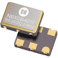
NBXDBA017LN1TAG ON Semiconductor, NBXDBA017LN1TAG Datasheet

IC CLK OSC LVPECL 3.3V 6-CLCC

NBXDBA017LN1TAG

Manufacturer Part Number
NBXDBA017LN1TAG
Description
IC CLK OSC LVPECL 3.3V 6-CLCC
Manufacturer
ON Semiconductor
Type
Clock Oscillatorr
Series
NBXr
Datasheet

Specifications of NBXDBA017LN1TAG

Package / Case
6-CLCC
Voltage - Supply
3 V ~ 3.6 V
Frequency
312.5MHz
Operating Temperature
-40°C ~ 85°C
Count
*
Product
XO
Frequency Stability
50 PPM
Supply Voltage
3.3 Volts
Termination Style
SMD/SMT
Minimum Operating Temperature
- 40 C
Maximum Operating Temperature
+ 85 C
Dimensions
5 mm W x 7 mm L
Height
1.8 mm
Duty Cycle (max)
52 %
Mounting Style
SMD/SMT
Supply Voltage (max)
3.63 Volts
Supply Voltage (min)
2.97 Volts
Lead Free Status / RoHS Status
Lead free / RoHS Compliant

Available stocks

Company
Part Number
Manufacturer
Quantity
Price
Part Number:
NBXDBA017LN1TAG
Manufacturer:
ON
Quantity:
1 000
NBXDBB017, NBXDBA017,
NBXHBA017, NBXSBA017
3.3 V, 156.25 MHz /
312.5 MHz LVPECL Clock
Oscillator
meet today’s requirements for 3.3 V LVPECL clock generation
applications. The device uses a high Q fundamental crystal and Phase
Lock Loop (PLL) multiplier to provide selectable 156.25 MHz or
312.5 MHz, ultra low jitter and phase noise LVPECL differential
output.
family that provides accurate and precision clock solutions.
and reel in quantities of 1,000. Frequency stability options available as
either 50 PPM NBXDBA017, NBXSBA017, NBXHBA017
(Industrial Temperature Range) or 20 PPM NBXDBB017
(Commercial Temperature Range).
Features
Applications
© Semiconductor Components Industries, LLC, 2009
October, 2009 − Rev. 3
The single and dual frequency crystal oscillator (XO) is designed to
This device is a member of ON Semiconductor’s PureEdget clock
Available in 5 mm x 7 mm SMD (CLCC) package on 16 mm tape
* NBXSBA017 and NBXHBA017 only
LVPECL Differential Output
Uses High Q Fundamental Mode Crystal and PLL Multiplier
Ultra Low Jitter and Phase Noise − 0.4 ps (12 kHz − 20 MHz)
Selectable Output Frequency − 156.25 MHz (default) / 312.5 MHz
Hermetically Sealed Ceramic SMD Package
RoHS Compliant
Operating Range 3.3 V ±10%
Total Frequency Stability − ±20 PPM or ±50 PPM
This is a Pb−Free Device
Networking
10 Gigabit Ethernet
Crystal
V
OE
DD
1
6
Figure 1. Simplified Logic Diagram
FSEL/NC*
Multiplier
Clock
PLL
2
CLK CLK
GND
5
3
4
1
See detailed ordering and shipping information in the package
dimensions section on page 7 of this data sheet.
AAWLYYWWG
AAWLYYWWG
156.25/312.5 = Output Frequency (MHz)
AA
WL
YY
WW
G
156.25/312.50
NBXDBA017
NBXSBA017
ORDERING INFORMATION
312.5
MARKING DIAGRAMS
http://onsemi.com
= Assembly Location
= Wafer Lot
= Year
= Work Week
= Pb−Free Package
Publication Order Number:
CASE 848AB
6 PIN CLCC
LN SUFFIX
AAWLYYWWG
AAWLYYWWG
156.25/312.50
NBXDBB017
NBXHBA017
156.25
NBXDBB017/D

Related parts for NBXDBA017LN1TAG

NBXDBA017LN1TAG Summary of contents

Page 1

... Lock Loop (PLL) multiplier to provide selectable 156.25 MHz or 312.5 MHz, ultra low jitter and phase noise LVPECL differential output. This device is a member of ON Semiconductor’s PureEdget clock family that provides accurate and precision clock solutions. Available SMD (CLCC) package tape and reel in quantities of 1,000 ...

Page 2

FSEL Table 1. PIN DESCRIPTION Pin No. Symbol I/O Á Á Á Á Á Á Á Á Á Á Á Á Á Á LVTTL/LVCMOS Control Input Á Á Á Á Á Á Á Á Á Á Á Á ...

Page 3

Table 6. DC CHARACTERISTICS (V Symbol Characteristic I Power Supply Current (Note and FSEL Input HIGH Voltage and FSEL Input LOW Voltage IL I Input HIGH Current IH I Input LOW Current IL ...

Page 4

Table 7. AC CHARACTERISTICS (V Symbol Characteristic f Output Clock Frequency CLKOUT Frequency Stability − NBXDBB017 Df − NBXDBA017/NBXSBA017/NBXHBA017 F Phase−Noise Performance NOISE f = 156.25 MHz/312.5 MHz CLKout (See Figures 3 and 4) RMS Phase Jitter t (F) jit ...

Page 5

Figure 3. Typical Phase Noise Plot at 156.25 MHz Figure 4. Typical Phase Noise Plot at 312.5 MHz http://onsemi.com 5 ...

Page 6

Table 8. RELIABILITY COMPLIANCE Parameter Á Á Á Á Á Á Á Á Á Á Á Shock Á Á Á Á Á Á Á Á Á Á Á Á Á Á Á Á Á Á Á Á Á Á Solderability ...

Page 7

... ORDERING INFORMATION Device Order Number NBXDBB017LN1TAG NBXDBA017LN1TAG NBXSBA017LN1TAG NBXHBA017LN1TAG* NBXDBB017LNHTAG NBXDBA017LNHTAG NBXSBA017LNHTAG NBXHBA017LNHTAG* †For information on tape and reel specifications, including part orientation and tape sizes, please refer to our Tape and Reel Packaging Specifications Brochure, BRD8011/D. *Please contact sales office for availability Package Type CLCC− ...

Page 8

... L 6X 2.54 PITCH *For additional information on our Pb−Free strategy and soldering details, please download the ON Semiconductor Soldering and Mounting Techniques Reference Manual, SOLDERRM/D. N. American Technical Support: 800−282−9855 Toll Free USA/Canada Europe, Middle East and Africa Technical Support: Phone: 421 33 790 2910 Japan Customer Focus Center Phone: 81− ...

Related keywords