DS4106BN+ Maxim Integrated Products, DS4106BN+ Datasheet

IC OSC CLOCK 106.25MHZ 10-LCCC

DS4106BN+

Manufacturer Part Number
DS4106BN+
Description
IC OSC CLOCK 106.25MHZ 10-LCCC
Manufacturer
Maxim Integrated Products
Type
Clock Oscillatorr
Datasheet

Specifications of DS4106BN+

Frequency
106.25MHz
Voltage - Supply
3 V ~ 3.6 V
Current - Supply
53mA
Operating Temperature
-40°C ~ 85°C
Package / Case
10-LCCC
Lead Free Status / RoHS Status
Lead free / RoHS Compliant
Count
-
The DS4106, DS4212, and DS4425 ceramic surface-
mount crystal oscillators are part of Maxim’s DS4-XO
series of crystal oscillators. These devices offer output
frequencies at 106.25MHz, 212.5MHz, and 425MHz.
The clock oscillators are suited for systems with tight tol-
erances because of the jitter, phase noise, and stability
performance. The small package provides a format
made for applications where PCB space is critical.
These clock oscillators are crystal based and use a fun-
damental crystal with PLL technology to provide the
final output frequencies. Each device is offered with
LVDS or LVPECL output types. The output enable pin is
active-high logic.
These clock oscillators have very low phase jitter and
phase noise. Typical phase jitter is < 0.9ps RMS from
12kHz to 20MHz. The devices are designed to operate
with a 3.3V ±10% supply voltage, and are available in a
5.0mm x 3.2mm x 1.49mm, 10-pin LCCC surface-mount
ceramic package.
Rev 2; 4/08
Pin Configuration and Selector Guide appear at end of
data sheet.
For pricing, delivery, and ordering information, please contact Maxim Direct at 1-888-629-4642,
or visit Maxim’s website at www.maxim-ic.com.
OE
Fibre Channel Hard Disk Drives
Host Bus Adapters
Raid Controllers
Fibre Channel Switches
DS4106/
DS4212/
DS4425
GND
V
V
CC
CC
OUTN
OUTP
________________________________________________________________ Maxim Integrated Products
LVPECL OPTION
General Description
50Ω
50Ω
V
CC
- 2V
100Ω
Applications
LVPECL
106.25MHz/212.5MHz/425MHz
V
CC
♦ Clock Output Frequencies:
♦ Phase Jitter (RMS): 0.9ps Typical
♦ LVPECL or LVDS Output
♦ Supply Current:
♦ -40°C to +85°C Temperature Range
♦ Output Disable
+ Denotes a lead(Pb)-free package. The lead finish is JESD97
category e4 (Au over Ni) and is compatible with both lead-based
and lead-free soldering processes.
DS4106AN+
DS4212AN+
DS4425AN+
DS4106BN+
DS4212BN+
DS4425BN+
OE
PART
DS4106: 106.25MHz
DS4212: 212.50MHz
DS4425: 425.00MHz
50mA (Typical, Unloaded) at +3.3V Supply
53mA (Typical) at +3.3V Supply (LVDS)
DS4106/
DS4212/
(LVPECL)
DS4425
GND
V
V
CC
CC
OUTN
OUTP
Typical Operating Circuits
Clock Oscillators
-40°C to +85°C
-40°C to +85°C
-40°C to +85°C
-40°C to +85°C
-40°C to +85°C
-40°C to +85°C
TEMP RANGE
LVDS OPTION
Ordering Information
100Ω
LVDS
PIN-PACKAGE
10 LCCC
10 LCCC
10 LCCC
10 LCCC
10 LCCC
10 LCCC
V
Features
CC
1

Related parts for DS4106BN+

DS4106BN+ Summary of contents

Page 1

... Unloaded) at +3.3V Supply (LVPECL) 53mA (Typical) at +3.3V Supply (LVDS) ♦ -40°C to +85°C Temperature Range ♦ Output Disable PART DS4106AN+ DS4106BN+ DS4212AN+ Applications DS4212BN+ DS4425AN+ DS4425BN+ + Denotes a lead(Pb)-free package. The lead finish is JESD97 category e4 (Au over Ni) and is compatible with both lead-based and lead-free soldering processes ...

Page 2

Clock Oscillators ABSOLUTE MAXIMUM RATINGS V , GND, OE, OUTP, OUTN .....................................-0.3V, +4V CC Operating Temperature Range ...........................-40°C to +85°C Junction Temperature ......................................................+150°C Stresses beyond those listed under “Absolute Maximum Ratings” may cause permanent damage to the device. These ...

Page 3

ELECTRICAL CHARACTERISTICS (continued 3.0V to 3.6V -40°C to +85°C, typical values are PARAMETER SYMBOL LVDS Change in V for OS Complementary States LVDS Differential Output R OLVDSO Impedance LVDS Output Current I ...

Page 4

Clock Oscillators ELECTRICAL CHARACTERISTICS (continued 3.0V to 3.6V -40°C to +85°C, typical values are PARAMETER SYMBOL Clock Output SSB Phase Noise Note 1: Limits at -40°C are guaranteed by design and ...

Page 5

PIN NAME Output Enable. On-chip pullup resistor. Connect OE to logic-high, V output clock. Connect OE to logic-low or GND to disable the output clock. The LVPECL output 1 OE clock is set to high impedance when disabled. The LVDS ...

Page 6

... OUTP SINGLE-ENDED OUTPUT OUTN DIFFERENTIAL 0V (DIFF) OUTPUT Figure 2. LVDS Level Definitions PART DS4106AN+ DS4106BN+ DS4212AN+ DS4212BN+ DS4425AN+ DS4425BN+ + Denotes a lead-free package. The lead finish is JESD97 category e4 (Au over Ni) and is compatible with both lead-based and lead- free soldering processes. 6 _______________________________________________________________________________________ RL = 100Ω ...
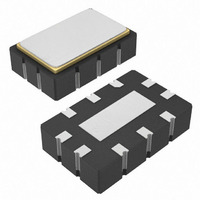
Page 7

Pin Configuration TOP VIEW N.C. N. DS4106/ DS4212/ N. OUTN DS4425 GND 3 *EP 4 OUTP N.C. N.C. (5.00mm × 3.20mm × 1.49mm) *EXPOSED PAD _______________________________________________________________________________________ Clock Oscillators Thermal Information THETA-JA ...

Page 8

... Maxim cannot assume responsibility for use of any circuitry other than circuitry entirely embodied in a Maxim product. No circuit patent licenses are implied. Maxim reserves the right to change the circuitry and specifications without notice at any time. 8 _____________________Maxim Integrated Products, 120 San Gabriel Drive, Sunnyvale, CA 94086 408-737-7600 © 2008 Maxim Integrated Products ...

Related keywords