DS4100HW+ Maxim Integrated Products, DS4100HW+ Datasheet - Page 2
DS4100HW+
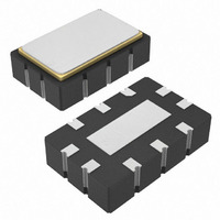
Manufacturer Part Number
DS4100HW+
Description
IC OSC CLOCK 100MHZ HCSL 10LCCC
Manufacturer
Maxim Integrated Products
Type
Clock Oscillatorr
Datasheet
1.DS4100H.pdf
(7 pages)
Specifications of DS4100HW+
Frequency
100MHz
Voltage - Supply
3.135 V ~ 3.465 V
Current - Supply
71mA
Operating Temperature
-40°C ~ 85°C
Package / Case
10-LCCC
Lead Free Status / RoHS Status
Lead free / RoHS Compliant
Count
-


ABSOLUTE MAXIMUM RATINGS
Power-Supply Voltage (V
Continuous Power Dissipation (T
Operating Temperature Range ...........................-40°C to +85°C
Junction Temperature ......................................................+150°C
100MHz HCSL Clock Oscillator
Stresses beyond those listed under “Absolute Maximum Ratings” may cause permanent damage to the device. These are stress ratings only, and functional
operation of the device at these or any other conditions beyond those indicated in the operational sections of the specifications is not implied. Exposure to
absolute maximum rating conditions for extended periods may affect device reliability.
ELECTRICAL CHARACTERISTICS
(V
2
Supply Voltage
Supply Current
Input High Voltage (OE)
Input Low Voltage (OE)
Input Leakage Current
(OE)
HCSL OUTPUTS (OUTP, OUTN)
Output High Current
Output High Voltage
Output Low Voltage
Output Leakage High
Current
Output Leakage Low
Current
Output Resistance
Crossover Voltage
Output Rise Time
Output Fall Time
Overshoot
Undershoot
Output-Enable Time to
Low Level
Output-Enable Time to
High Level
CC
_______________________________________________________________________________________
= 3.135V to 3.465V, T
PARAMETER
CC
A
) .......................................-0.3V, +4V
SYMBOL
I_
I_
V
V
V
= -40°C to +85°C. Typical values are at V
CROSS
UNDER
LEAKH
V
LEAKL
t
V
V
t
OVER
I
V
I
R
PZH
V
PZL
I
CC
OH
t
t
CC
OH
IN
OL
R
IH
F
IL
A
O
= +70°C) ...................280mW
(Note 1)
OE = V
(Note 1)
(Note 1)
GND
475
or V
R
R
V
V
Measure current out of OUTN pin at V
R
Measure crossing voltage at OUTP and OUTN
(Notes 1, 2, and 3)
20% to 80%, CL = 2pF
80% to 20%, CL = 2pF
Measure overshoot voltage at OUTP and OUTN
(Notes 1, 2, and 3)
Measure undershoot voltage at OUTP and OUTN
(Notes 1, 2, and 3)
Figure 3 (Note 4)
Figure 3 (Note 5)
OE
OE
S
S
O
= 0 , R
= 0 , R
= 0.5 / I
OUTP
= 0; V
= 0; V
resistor connected between RREF and GND, V
IH
OE
, Figure 2
= 1.2V, V
OUTN
OUTN
T
T
0.5
V
= 50
= 50
CC
- I
, V
, V
1.0
OUTP
OUTP
CC
(Notes 1, 2)
(Notes 1, 2)
= 3.3V ±5%
CONDITIONS
= V
= 0
CC
Storage Temperature Range ...............................-40°C to +85°C
Soldering Temperature Profile
CC
(3 passes max) .......................................................Refer to the
= +3.3V and T
OUTN
= 0.5V and 1.0V;
A
= +25°C, unless otherwise noted.)
OUTN
IPC/JEDEC J-STD-020 specification.
3.135 3.300 3.465
12.25 13.92 15.59
612.5 696.0 779.5
3000
MIN
175
175
2.0
-55
-10
-10
0
V
OH
(50% x
V
TYP
0.2V
-0.2
OH
71
) ±5%
0
+
MAX UNITS
V
+10
+10
+10
700
700
200
200
0.8
85
50
CC
mA
mA
mV
mV
mV
μA
μA
μA
ps
ps
ns
ns
V
V
V
V
V
Related parts for DS4100HW+
Image
Part Number
Description
Manufacturer
Datasheet
Request
R

Part Number:
Description:
IC OSC CLOCK 250MHZ 10-LCCC
Manufacturer:
Maxim Integrated Products
Datasheet:
Part Number:
Description:
IC OSC CLOCK 150MHZ 10-LCCC
Manufacturer:
Maxim Integrated Products
Datasheet:
Part Number:
Description:
IC OSC CLOCK 160MHZ 10-LCCC
Manufacturer:
Maxim Integrated Products
Datasheet:
Part Number:
Description:
IC OSC CLOCK 160MHZ 10-LCCC
Manufacturer:
Maxim Integrated Products
Datasheet:
Part Number:
Description:
IC OSC CLOCK 155.52MHZ 10-LCCC
Manufacturer:
Maxim Integrated Products
Datasheet:
Part Number:
Description:
IC OSC CLOCK 156.25MHZ 10-LCCC
Manufacturer:
Maxim Integrated Products
Datasheet:
Part Number:
Description:
IC OSC CLOCK 125MHZ 10-LCCC
Manufacturer:
Maxim Integrated Products
Datasheet:
Part Number:
Description:
IC OSC CLOCK 155.52MHZ 10-LCCC
Manufacturer:
Maxim Integrated Products
Datasheet:
Part Number:
Description:
IC OSC CLOCK 156.25MHZ 10-LCCC
Manufacturer:
Maxim Integrated Products
Datasheet:
Part Number:
Description:
IC OSC CLOCK 150MHZ 10-LCCC
Manufacturer:
Maxim Integrated Products
Datasheet:
Part Number:
Description:
IC OSC CLOCK 300MHZ 10-LCCC
Manufacturer:
Maxim Integrated Products
Datasheet:
Part Number:
Description:
IC OSC CLOCK 300MHZ 10-LCCC
Manufacturer:
Maxim Integrated Products
Datasheet:
Part Number:
Description:
IC OSC CLOCK 250MHZ 10-LCCC
Manufacturer:
Maxim Integrated Products
Datasheet:

Part Number:
Description:
MAX7528KCWPMaxim Integrated Products [CMOS Dual 8-Bit Buffered Multiplying DACs]
Manufacturer:
Maxim Integrated Products
Datasheet:
Part Number:
Description:
Single +5V, fully integrated, 1.25Gbps laser diode driver.
Manufacturer:
Maxim Integrated Products
Datasheet: