DS4M133D+33 Maxim Integrated Products, DS4M133D+33 Datasheet - Page 6
DS4M133D+33
Manufacturer Part Number
DS4M133D+33
Description
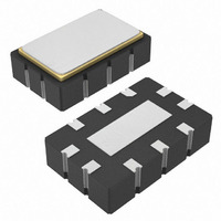
IC OSC CLOCK 133.33MHZ 10-LCCC
Manufacturer
Maxim Integrated Products
Type
Clock Oscillatorr
Datasheet
1.DS4M133D33.pdf
(7 pages)
Specifications of DS4M133D+33
Frequency
133.33MHz
Voltage - Supply
3.135 V ~ 3.465 V
Current - Supply
74mA
Operating Temperature
-40°C ~ 85°C
Package / Case
10-LCCC
Lead Free Status / RoHS Status
Lead free / RoHS Compliant
Count
-


3.3V Margining Clock Oscillator with
LVPECL/LVDS Output
The DS4M125/DS4M133/DS4M200 consist of an oscil-
lator designed to oscillate with a fundamental-mode
crystal and a PLL to synthesize the base frequency with
its ±5% deviations. The output interface is either
LVPECL or LVDS.
The ±5% frequency deviation is controlled through a
three-level margining select (MS) pin. This three-state
input pin accepts a three-level voltage signal to control
the output frequency. In a low-level state, the output
frequency is set to the nominal frequency. When set to
a high-level state, the frequency output is set to the
Figure 1. Functional Diagram
Figure 2. LVDS Output Timing Diagram When OE Is Enabled
and Disabled
6
MS
_______________________________________________________________________________________
OUTN
OUTP
OE
0.7 x V
X1
X2
GND
CC
DS4M125/
DS4M133/
DS4M200
t
DECODER
P1A
THREE-
LEVEL
Detailed Description
THREE-
PHASE
STATE
DET
t
FILTER
PA1
0.3 x V
CC
DIVFB
LC-VCO
nominal frequency plus 5%. When set to the mid-level
state, the frequency output is equal to the nominal fre-
quency minus 5%. The MS pin has an internal 100kΩ
pulldown resistor. When the pin is left floating, the
devices output a nominal frequency.
The devices are available with either LVDS or LVPECL
output drivers. When the OE signal is low, the LVPECL
output driver is turned off and the output voltage goes
to the PECL_BIAS level of V
outputs are a logical one. The OE pin has an internal
100kΩ pullup resistor. When the pin is left floating, the
device output is active.
Figure 3. LVPECL Output Timing Diagram When OE Is Enabled
and Disabled
DIVP
OUTN
OUTP
FREQUENCY SELECTION
OE
0.7 x V
PECL_BIAS
PECL_BIAS
CC
DIVOUT
t
PZA
OUTSELN
CC
- 2.0V, while the LVDS
OUTDRV
VCC
0.3 x V
t
PAZ
PECL_BIAS
PECL_BIAS
CC
OE
OUTP
OUTN
Related parts for DS4M133D+33
Image
Part Number
Description
Manufacturer
Datasheet
Request
R

Part Number:
Description:
3.3v Margining Clock Oscillator With Lvpecl/lvds Output
Manufacturer:
Maxim Integrated Products, Inc.
Datasheet:

Part Number:
Description:
MAX7528KCWPMaxim Integrated Products [CMOS Dual 8-Bit Buffered Multiplying DACs]
Manufacturer:
Maxim Integrated Products
Datasheet:
Part Number:
Description:
Single +5V, fully integrated, 1.25Gbps laser diode driver.
Manufacturer:
Maxim Integrated Products
Datasheet:
Part Number:
Description:
Single +5V, fully integrated, 155Mbps laser diode driver.
Manufacturer:
Maxim Integrated Products
Datasheet:
Part Number:
Description:
VRD11/VRD10, K8 Rev F 2/3/4-Phase PWM Controllers with Integrated Dual MOSFET Drivers
Manufacturer:
Maxim Integrated Products
Datasheet:
Part Number:
Description:
Highly Integrated Level 2 SMBus Battery Chargers
Manufacturer:
Maxim Integrated Products
Datasheet:
Part Number:
Description:
Current Monitor and Accumulator with Integrated Sense Resistor; ; Temperature Range: -40°C to +85°C
Manufacturer:
Maxim Integrated Products
Part Number:
Description:
TSSOP 14/A�/RS-485 Transceivers with Integrated 100O/120O Termination Resis
Manufacturer:
Maxim Integrated Products
Part Number:
Description:
TSSOP 14/A�/RS-485 Transceivers with Integrated 100O/120O Termination Resis
Manufacturer:
Maxim Integrated Products
Part Number:
Description:
QFN 16/A�/AC-DC and DC-DC Peak-Current-Mode Converters with Integrated Step
Manufacturer:
Maxim Integrated Products
Part Number:
Description:
TDFN/A/65V, 1A, 600KHZ, SYNCHRONOUS STEP-DOWN REGULATOR WITH INTEGRATED SWI
Manufacturer:
Maxim Integrated Products
Part Number:
Description:
Integrated Temperature Controller f
Manufacturer:
Maxim Integrated Products
Part Number:
Description:
SOT23-6/I�/45MHz to 650MHz, Integrated IF VCOs with Differential Output
Manufacturer:
Maxim Integrated Products
Part Number:
Description:
SOT23-6/I�/45MHz to 650MHz, Integrated IF VCOs with Differential Output
Manufacturer:
Maxim Integrated Products
Part Number:
Description:
EVALUATION KIT/2.4GHZ TO 2.5GHZ 802.11G/B RF TRANSCEIVER WITH INTEGRATED PA
Manufacturer:
Maxim Integrated Products