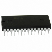
M48T08-150PC1 STMicroelectronics, M48T08-150PC1 Datasheet - Page 10

M48T08-150PC1
Manufacturer Part Number
M48T08-150PC1
Description
IC TIMEKPR NVRAM 64KBIT 5V 28-DI
Manufacturer
STMicroelectronics
Series
Timekeeper®r
Type
Clock/Calendar/NVSRAMr
Specifications of M48T08-150PC1
Memory Size
64K (8K x 8)
Time Format
HH:MM:SS (24 hr)
Date Format
YY-MM-DD-dd
Interface
Parallel
Voltage - Supply
4.75 V ~ 5.5 V
Operating Temperature
0°C ~ 70°C
Mounting Type
Through Hole
Package / Case
28-DIP Module (600 mil), 28-EDIP
Function
Clock/Calendar/NV Timekeeping RAM/Battery Backup
Rtc Memory Size
8192 Byte
Supply Voltage (max)
5.5 V
Supply Voltage (min)
4.75 V
Maximum Operating Temperature
+ 70 C
Minimum Operating Temperature
0 C
Mounting Style
Through Hole
Rtc Bus Interface
Parallel
Capacitance, Input
10 pF
Capacitance, Output
10 pF
Current, Input, Leakage
±1 μA
Current, Operating
80 mA
Current, Output, Leakage
±1
Data Retention
10 yrs.
Density
64K
Memory Type
Non-Volatile SRAM
Organization
8K×8
Package Type
PCDIP28
Power Dissipation
1 W
Temperature, Operating
0 to +70 °C
Time, Access
150 ns
Time, Fall
≤5 ns
Time, Rise
≤5 ns
Voltage, Input, High
5.05 to 5.8 V
Voltage, Input, Low
0.8 V
Voltage, Output, High
2.4 V
Voltage, Output, Low
0.4 V
Voltage, Supply
4.75 to 5.5 V
Lead Free Status / RoHS Status
Lead free / RoHS Compliant
Other names
497-2829-5
Available stocks
Company
Part Number
Manufacturer
Quantity
Price
Company:
Part Number:
M48T08-150PC1
Manufacturer:
ST
Quantity:
120
Part Number:
M48T08-150PC1
Manufacturer:
ST
Quantity:
20 000
Operation modes
Table 3.
Note:
2.2
10/31
Symbol
t
t
t
t
t
t
t
t
t
t
t
E2HQV
E2HQX
E1HQZ
t
E1LQV
E1LQX
E2LQZ
GHQZ
AVQV
GLQV
GLQX
AXQX
AVAV
READ mode AC characteristics
Valid for ambient operating temperature: T
(except where noted).
WRITE mode
The M48T08/18/08Y is in the WRITE mode whenever W, E1, and E2 are active. The start of
a WRITE is referenced from the latter occurring falling edge of W or E1, or the rising edge of
E2. A WRITE is terminated by the earlier rising edge of W or E1, or the falling edge of E2.
The addresses must be held valid throughout the cycle. E1 or W must return high or E2 low
for a minimum of t
initiation of another READ or WRITE cycle. Data-in must be valid t
WRITE and remain valid for t
avoid bus contention; however, if the output bus has been activated by a low on E1 and G
and a high on E2, a low on W will disable the outputs t
READ cycle time
Address valid to output valid
Chip enable 1 low to output valid
Chip enable 2 high to output valid
Output enable low to output valid
Chip enable 1 low to output transition
Chip enable 2 high to output transition
Output enable low to output transition
Chip enable 1 high to output Hi-Z
Chip enable 2 low to output Hi-Z
Output enable high to output Hi-Z
Address transition to output transition
Parameter
E1HAX
or t
(1)
E2LAX
WHDX
Doc ID 2411 Rev 10
from chip enable or t
afterward. G should be kept high during WRITE cycles to
A
= 0 to 70 °C; V
–100/–10 (T08Y)
Min
100
10
10
5
5
M48T08/M48T18/T08Y
WHAX
WLQZ
Max
100
100
100
50
50
50
40
CC
from WRITE enable prior to the
after W falls.
= 4.75 to 5.5 V or 4.5 to 5.5 V
M48T08, M48T08Y, M48T18
–150/–15 (T08Y)
DVWH
Min
150
10
10
5
5
prior to the end of
Max
150
150
150
75
60
75
75
Unit
ns
ns
ns
ns
ns
ns
ns
ns
ns
ns
ns
ns


