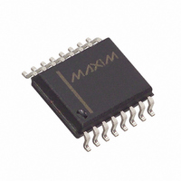
DS3231SN# Maxim Integrated Products, DS3231SN# Datasheet - Page 14

DS3231SN#
Manufacturer Part Number
DS3231SN#
Description
IC RTC W/TCXO 16-SOIC
Manufacturer
Maxim Integrated Products
Type
Clock/Calendar/TCXO/Crystalr
Datasheet
1.DS3231S.pdf
(20 pages)
Specifications of DS3231SN#
Time Format
HH:MM:SS (12/24 hr)
Date Format
YY-MM-DD-dd
Interface
I²C, 2-Wire Serial
Voltage - Supply
2.3 V ~ 5.5 V
Operating Temperature
-40°C ~ 85°C
Mounting Type
Surface Mount
Package / Case
16-SOIC (0.300", 7.5mm Width)
Function
Clock/Calendar/Battery Backup
Supply Voltage (max)
5.5 V
Supply Voltage (min)
2.3 V
Maximum Operating Temperature
+ 85 C
Minimum Operating Temperature
- 40 C
Mounting Style
SMD/SMT
Rtc Bus Interface
Serial (I2C)
Lead Free Status / RoHS Status
Lead free / RoHS Compliant
Memory Size
-
Lead Free Status / Rohs Status
Lead free / RoHS Compliant
Available stocks
Company
Part Number
Manufacturer
Quantity
Price
Bit 7: Oscillator Stop Flag (OSF). A logic 1 in this bit
indicates that the oscillator either is stopped or was
stopped for some period and may be used to judge the
validity of the timekeeping data. This bit is set to logic 1
any time that the oscillator stops. The following are exam-
ples of conditions that can cause the OSF bit to be set:
1) The first time power is applied.
2) The voltages present on both V
3) The EOSC bit is turned off in battery-backed mode.
4) External influences on the crystal (i.e., noise, leak-
This bit remains at logic 1 until written to logic 0.
Bit 3: Enable 32kHz Output (EN32kHz). This bit con-
trols the status of the 32kHz pin. When set to logic 1, the
32kHz pin is enabled and outputs a 32.768kHz square-
wave signal. When set to logic 0, the 32kHz pin goes to
a high-impedance state. The initial power-up state of
this bit is logic 1, and a 32.768kHz square-wave signal
appears at the 32kHz pin after a power source is
applied to the DS3231 (if the oscillator is running).
Bit 2: Busy (BSY). This bit indicates the device is busy
executing TCXO functions. It goes to logic 1 when the
conversion signal to the temperature sensor is asserted
and then is cleared when the device is in the 1-minute
idle state.
Bit 1: Alarm 2 Flag (A2F). A logic 1 in the alarm 2 flag
bit indicates that the time matched the alarm 2 regis-
ters. If the A2IE bit is logic 1 and the INTCN bit is set to
logic 1, the INT/SQW pin is also asserted. A2F is
cleared when written to logic 0. This bit can only be
written to logic 0. Attempting to write to logic 1 leaves
the value unchanged.
Bit 0: Alarm 1 Flag (A1F). A logic 1 in the alarm 1 flag
bit indicates that the time matched the alarm 1 regis-
Extremely Accurate I
RTC/TCXO/Crystal
14
insufficient to support oscillation.
age, etc.).
NAME:
NAME:
POR:
POR:
____________________________________________________________________
BIT 7
BIT 7
Sign
OSF
1
0
Status Register (0Fh)
BIT 6
BIT 6
Data
0
0
0
CC
and V
BIT 5
BIT 5
Data
0
0
0
BAT
2
are
C-Integrated
BIT 4
BIT 4
Data
0
0
0
ters. If the A1IE bit is logic 1 and the INTCN bit is set to
logic 1, the INT/SQW pin is also asserted. A1F is
cleared when written to logic 0. This bit can only be
written to logic 0. Attempting to write to logic 1 leaves
the value unchanged.
The aging offset register takes a user-provided value to
add to or subtract from the codes in the capacitance
array registers. The code is encoded in two’s comple-
ment, with bit 7 representing the sign bit. One LSB rep-
resents one small capacitor to be switched in or out of
the capacitance array at the crystal pins. The aging off-
set register capacitance value is added or subtracted
from the capacitance value that the device calculates
for each temperature compensation. The offset register
is added to the capacitance array during a normal tem-
perature conversion, if the temperature changes from
the previous conversion, or during a manual user con-
version (setting the CONV bit). To see the effects of the
aging register on the 32kHz output frequency immedi-
ately, a manual conversion should be started after each
aging register change.
Positive aging values add capacitance to the array,
slowing the oscillator frequency. Negative values
remove capacitance from the array, increasing the
oscillator frequency.
The change in ppm per LSB is different at different
temperatures. The frequency vs. temperature curve is
shifted by the values used in this register. At +25°C,
one LSB typically provides about 0.1ppm change in
frequency.
Use of the aging register is not needed to achieve the
accuracy as defined in the EC tables, but could be
used to help compensate for aging at a given tempera-
ture. See the Typical Operating Characteristics section
for a graph showing the effect of the register on accu-
racy over temperature.
EN32kHz
BIT 3
BIT 3
Data
1
0
BIT 2
BIT 2
Data
BSY
X
0
Status Register (0Fh)
Aging Offset (10h)
BIT 1
BIT 1
Data
A2F
Aging Offset
X
0
BIT 0
BIT 0
Data
A1F
X
0


