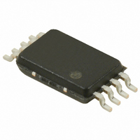
S-35190A-T8T1G Seiko Instruments, S-35190A-T8T1G Datasheet - Page 30

S-35190A-T8T1G
Manufacturer Part Number
S-35190A-T8T1G
Description
IC REAL TIME CLOCK 3WIRE 8-TSSOP
Manufacturer
Seiko Instruments
Type
Clock/Calendarr
Datasheet
1.S-35190A-J8T1G.pdf
(55 pages)
Specifications of S-35190A-T8T1G
Time Format
HH:MM:SS (12/24 hr)
Date Format
YY-MM-DD-dd
Interface
3-Wire Serial
Voltage - Supply
1.3 V ~ 5.5 V
Operating Temperature
-40°C ~ 85°C
Mounting Type
Surface Mount
Package / Case
8-TSSOP
Function
Clock/Calendar/Alarm/Battery Backup/Interrupt
Supply Voltage (max)
5.5 V
Supply Voltage (min)
1.3 V
Maximum Operating Temperature
+ 85 C
Minimum Operating Temperature
- 40 C
Mounting Style
SMD/SMT
Rtc Bus Interface
Serial (3-Wire)
Lead Free Status / RoHS Status
Lead free / RoHS Compliant
Memory Size
-
Lead Free Status / Rohs Status
Lead free / RoHS Compliant
Available stocks
Company
Part Number
Manufacturer
Quantity
Price
Part Number:
S-35190A-T8T1G
Manufacturer:
SEIKO
Quantity:
20 000
30
3-WIRE REAL-TIME CLOCK
S-35190A
Serial Interface
The S-35190A receives various commands via 3-wire serial interface to Read/Write data. Regarding transmission is as
follows.
1. Data Read
2. Data Write
3. Data access
When data is input from the SIO pin in synchronization with the falling of the SCK clock after setting the CS pin to “H”, the
data is loaded internally in synchronization with the next rising of the SCK clock. When
eighth rising of the SCK clock, the state of data reading is entered. Data corresponding to each command is then output
in synchronization with the falling of the subsequent SCK clock input. When the SCK clock is less than 8, the IC is in
the clock-wait status, and no processing is performed.
When data is input from the SIO pin in synchronization with the falling of the SCK clock after setting the CS pin to “H”, the
data is loaded internally in synchronization with the next rising of the SCK clock. When
eighth rising of the SCK clock, the state of data writing is entered. In this state, the data, which is input in synchronization
with the falling of the subsequent SCK clock input, is written to registers according to each command. In data Write, input
a clock pulse which is equivalent to the byte of the register. As well as in Read, when the SCK clock is less than 8, the IC
is in the clock-wait status, and no processing is performed.
(1) Real-time data 1 access
SCK
SIO
CS
X
0
1
1
Fixed code +
command
1
0
0
1
0
8
B7
R / W
Year data
Figure 34 Real-Time Data Access 1
During reading: Output mode switching
B0
Seiko Instruments Inc.
16
56
B7
Second data
R
R
During reading:
Input mode switching
/
/
W
W
64
B0
bit = “1” is loaded at the
bit = “0” is loaded at the
Rev.3.0
_00


