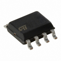
M41T00M6E STMicroelectronics, M41T00M6E Datasheet - Page 14

M41T00M6E
Manufacturer Part Number
M41T00M6E
Description
IC RTC SERIAL 8SOIC
Manufacturer
STMicroelectronics
Type
Clock/Calendar/NVSRAMr
Specifications of M41T00M6E
Memory Size
8B
Time Format
HH:MM:SS (24 hr)
Date Format
YY-MM-DD-dd
Interface
I²C, 2-Wire Serial
Voltage - Supply
2 V ~ 5.5 V
Operating Temperature
-40°C ~ 85°C
Mounting Type
Surface Mount
Package / Case
8-SOIC (3.9mm Width)
Function
Clock/Calendar/Battery Backup
Rtc Memory Size
8 Byte
Supply Voltage (max)
5.5 V
Supply Voltage (min)
2 V
Maximum Operating Temperature
+ 85 C
Minimum Operating Temperature
- 40 C
Mounting Style
SMD/SMT
Rtc Bus Interface
Serial (2-Wire, I2C)
Nvram Features
RTC, Internal Battery, XTAL
Interface Type
I2C, Serial
Supply Voltage Range
2V To 5.5V
Memory Case Style
SOIC
No. Of Pins
8
Operating Temperature Range
-40°C To
Rohs Compliant
Yes
Lead Free Status / RoHS Status
Contains lead / RoHS non-compliant
Other names
497-2810-5
M41T00M6
M41T00M6
Available stocks
Company
Part Number
Manufacturer
Quantity
Price
Company:
Part Number:
M41T00M6E
Manufacturer:
AVAGO
Quantity:
1 000
Part Number:
M41T00M6E
Manufacturer:
ST
Quantity:
20 000
3
Note:
Note:
14/25
M41T00 clock operation
The eight byte clock register (see
and time from the clock, in a binary coded decimal format. Seconds, minutes, and hours are
contained within the first three registers. Bits D6 and D7 of clock register 2 (century/hours
register) contain the century enable bit (CEB) and the century bit (CB). Setting CEB to a '1'
will cause CB to toggle, either from '0' to '1' or from '1' to '0' at the turn of the century
(depending upon its initial state). If CEB is set to a '0', CB will not toggle. Bits D0 through D2
of register 3 contain the day (day of week). Registers 4, 5 and 6 contain the date (day of
month), month and years. The final register is the control register (this is described in the
clock calibration section). Bit D7 of register 0 contains the STOP bit (ST). Setting this bit to a
'1' will cause the oscillator to stop. If the device is expected to spend a significant amount of
time on the shelf, the oscillator may be stopped to reduce current drain. When reset to a '0'
the oscillator restarts within one second.
In order to guarantee oscillator start-up after the initial power-up, set the ST bit to a '1,' then
reset this bit to a '0.' This sequence enables a “kick start” circuit which aids the oscillator
start-up during worst case conditions of voltage and temperature.
The seven clock registers may be read one byte at a time, or in a sequential block. The
control register (address location 7) may be accessed independently. Provision has been
made to ensure that a clock update does not occur while any of the seven clock addresses
are being read. If a clock address is being read, an update of the clock registers will be
delayed by 250 ms to allow the read to be completed before the update occurs. This will
prevent a transition of data during the read.
Note: This 250 ms delay affects only the clock register update and does not alter the actual
clock time.
Table
5) is used to both set the clock and to read the date


