DP8573AVX/NOPB National Semiconductor, DP8573AVX/NOPB Datasheet - Page 9
DP8573AVX/NOPB
Manufacturer Part Number
DP8573AVX/NOPB
Description
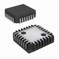
IC REAL TIME CLOCK (RTC) 28-PLCC
Manufacturer
National Semiconductor
Type
Clock/Calendar/NVSRAMr
Datasheet
1.DP8573AVXNOPB.pdf
(16 pages)
Specifications of DP8573AVX/NOPB
Memory Size
32B
Time Format
HH:MM:SS:hh (12/24 hr)
Date Format
YY-MM-DD-dd
Interface
Parallel
Voltage - Supply
4.5 V ~ 5.5 V
Operating Temperature
-40°C ~ 85°C
Mounting Type
Surface Mount
Package / Case
28-PLCC
Bus Type
Parallel
Operating Supply Voltage (typ)
5V
Package Type
PLCC
Operating Supply Voltage (max)
5.5V
Operating Supply Voltage (min)
4.5V
Operating Temperature Classification
Industrial
Operating Temperature (max)
85C
Operating Temperature (min)
-40C
Pin Count
28
Mounting
Surface Mount
Lead Free Status / RoHS Status
Lead free / RoHS Compliant
Other names
*DP8573AVX
*DP8573AVX/NOPB
DP8573AVX
*DP8573AVX/NOPB
DP8573AVX
Available stocks
Company
Part Number
Manufacturer
Quantity
Price
Company:

Part Number:
DP8573AVX/NOPB
Manufacturer:
Texas Instruments
Quantity:
10 000


Functional Description
POWER FAIL INTERRUPTS DESCRIPTION
The Power Fail Status Flag in the Main Status Register
monitors the state of the internal power fail signal This flag
may be interrogated by the P but it cannot be cleared it is
cleared automatically by the RTC when system power is
restored To generate an interrupt when the power fails the
Power Fail Interrupt Enable bit in Interrupt Control Register
1 is set Although this interrupt may not be cleared it may
be masked by clearing the Power Fail Interrupt Enable bit
POWER FAILURE CIRCUITRY FUNCTIONAL
DESCRIPTION
Since the clock must be operated from a battery when the
main system supply has been turned off the DP8573A pro-
vides circuitry to simplify design in battery backed systems
This switches over to the back up supply and isolates itself
from the host system Figure 6 shows a simplified block
diagram of this circuitry which consists of three major sec-
tions 1) power loss logic 2) battery switch over logic and 3)
isolation logic
Detection of power loss occurs when PFAIL is low De-
bounce logic provides a 30 s– 63 s debounce time which
will prevent noise on the PFAIL pin from being interpreted
as a system failure After 30 s– 63 s the debounce logic
times out and a signal is generated indicating that system
power is marginal and is failing The Power Fail Interrupt will
then be generated
If chip select is low when a power failure is detected a
safety circuit will ensure that if a read or write is held active
continuously for greater than 30 s after the power fail sig-
nal is asserted the lock-out will be forced
The battery switch over circuitry is completely independent
of the PFAIL pin A separate circuit compares V
V
to operate from the V
voltage At this time the battery supply is switched in V
BB
voltage As the main supply fails the RTC will continue
CC
pin until V
FIGURE 6 System-Battery Switchover (Upper Left) Power Fail
CC
(Continued)
falls below the V
and Lock-Out Circuits (Lower Right)
CC
to the
CC
BB
is
9
disconnected and the device is now in the standby mode If
indeterminate operation of the battery switch over circuit is
to be avoided then the voltage at the V
allowed to equal the voltage at the V
After the generation of a lock-out signal and eventual
switch in of the battery supply the pins of the RTC will be
configured as shown in Table II Outputs that have a pull-up
resistor should be connected to a voltage no greater than
V
The Interrupt Power Fail Operation bit in the Real-Time
Mode Register determines whether or not the interrupts will
continue to function after a power fail event
As power returns to the system the battery switch over cir-
cuit will switch back to V
greater than the battery voltage The chip will remain in the
locked out state as long as PFAIL
chip is unlocked but only after another 30 s min
that his system is stable when power has returned
The power fail circuitry contains active linear circuitry that
draws supply current from V
undesirable so this circuit can be disabled by masking the
power fail interrupt The power fail input can perform all
lock-out functions previously mentioned except that no ex-
BB
s max debounce time The system designer must ensure
CS RD WR
INTR MFO
Oscillator
TABLE II Pin Isolation during a Power Failure
D0– D7
A0– A4
PFAIL
Pin
Locked Out
Locked Out
Locked Out
Not Isolated
Not Isolated
Not Isolated
PFAIL
Logic 0
CC
CC
power as soon as it becomes
e
In some cases this may be
e
0 When PFAIL
BB
CC
pin
Standby Mode
Locked Out
Locked Out
Locked Out
Not Isolated
Not Isolated
Open Drain
V
pin must not be
BB l
TL F 9981 – 11
V
CC
e
1 the
63
Related parts for DP8573AVX/NOPB
Image
Part Number
Description
Manufacturer
Datasheet
Request
R

Part Number:
Description:
IC REAL TIME CLOCK (RTC) 28-PLCC
Manufacturer:
National Semiconductor
Datasheet:

Part Number:
Description:
Clock IC
Manufacturer:
National Semiconductor
Datasheet:

Part Number:
Description:
National Semiconductor [8-Bit D/A Converter]
Manufacturer:
National Semiconductor
Datasheet:
Part Number:
Description:
National Semiconductor [Media Coprocessor]
Manufacturer:
National Semiconductor
Datasheet:
Part Number:
Description:
Digitally Controlled Tone and Volume Circuit with Stereo Audio Power Amplifier, Microphone Preamp Stage and National 3D Sound
Manufacturer:
National Semiconductor
Datasheet:
Part Number:
Description:
Digitally Controlled Tone and Volume Circuit with Stereo Audio Power Amplifier, Microphone Preamp Stage and National 3D Sound
Manufacturer:
National Semiconductor
Datasheet:
Part Number:
Description:
AC97 Rev 2 Codec with Sample Rate Conversion and National 3D Sound
Manufacturer:
National Semiconductor
Part Number:
Description:
Manufacturer:
National Semiconductor
Datasheet:
Part Number:
Description:
Manufacturer:
National Semiconductor
Datasheet:
Part Number:
Description:
General Purpose, Low Voltage, Low Power, Rail-to-Rail Output Operational Amplifiers
Manufacturer:
National Semiconductor
Datasheet:
Part Number:
Description:
8-bit 20 MSPS flash A/D converter.
Manufacturer:
National Semiconductor
Datasheet:
Part Number:
Description:
Low Noise Quad Operational Amplifier
Manufacturer:
National Semiconductor
Datasheet:
Part Number:
Description:
Quad Differential Line Receivers
Manufacturer:
National Semiconductor
Datasheet: