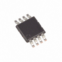
DS1371U+C01 Maxim Integrated Products, DS1371U+C01 Datasheet - Page 13

DS1371U+C01
Manufacturer Part Number
DS1371U+C01
Description
IC BINARY COUNTER 32-BIT 8-USOP
Manufacturer
Maxim Integrated Products
Type
Binary Counterr
Datasheet
1.DS1371U.pdf
(15 pages)
Specifications of DS1371U+C01
Time Format
Binary
Date Format
Binary
Interface
I²C, 2-Wire Serial
Voltage - Supply
1.7 V ~ 5.5 V
Operating Temperature
-40°C ~ 85°C
Mounting Type
Surface Mount
Package / Case
8-MSOP, Micro8™, 8-uMAX, 8-uSOP,
Lead Free Status / RoHS Status
Lead free / RoHS Compliant
Memory Size
-
Figures 5 and 6 detail how data transfer is accomplished on the I
R/W bit, two types of data transfer are possible:
The DS1371 can operate in the following two modes:
Data transfer from a master transmitter to a slave receiver. The first byte transmitted by the
master is the slave address. Next follows a number of data bytes. The slave returns an
acknowledge bit after each received byte.
Data transfer from a slave transmitter to a master receiver. The first byte (the slave address)
is transmitted by the master. The slave then returns an acknowledge bit. Next follows a number of
data bytes transmitted by the slave to the master. The master returns an acknowledge bit after all
received bytes other than the last byte. At the end of the last received byte, a “not acknowledge” is
returned.
The master device generates all of the serial clock pulses and the START and STOP conditions. A
transfer is ended with a STOP condition or with a repeated START condition. Since a repeated
START condition is also the beginning of the next serial transfer, the bus is not released.
Slave receiver mode (DS1371 write mode). Serial data and clock are received through SDA and
SCL. After each byte is received, an acknowledge bit is transmitted. START and STOP conditions
are recognized as the beginning and end of a serial transfer. Address recognition is performed by
hardware after reception of the slave address and direction bit. The slave address byte is the first
byte received after the START condition is generated by the master. The slave address byte
contains the 7-bit DS1371 address, which is 1101000, followed by the direction bit (R/W), which
for a write is a 0. After receiving and decoding the slave address byte the DS1371 outputs an
acknowledge on SDA. After the DS1371 acknowledges the slave address + write bit, the master
transmits a word address to the DS1371. This sets the register pointer on the DS1371, with the
DS1371 acknowledging the transfer. The master may then transmit zero or more bytes of data,
with the DS1371 acknowledging each byte received. The register pointer increments after each
byte is transferred. The master generates a STOP condition to terminate the data write.
Slave transmitter mode (DS1371 read mode). The first byte is received and handled as in the
slave receiver mode. However, in this mode, the direction bit indicates that the transfer direction is
reversed. Serial data is transmitted on SDA by the DS1371 while the serial clock is input on SCL.
START and STOP conditions are recognized as the beginning and end of a serial transfer.
Address recognition is performed by hardware after reception of the slave address and direction
bit. The slave address byte is the first byte received after the START condition is generated by the
master. The slave address byte contains the 7-bit DS1371 address, which is 1101000, followed by
the direction bit (R/W), which for a read is a 1. After receiving and decoding the slave address
byte, the DS1371 outputs an acknowledge on SDA. The DS1371 then begins to transmit data
starting with the register address pointed to by the register pointer. If the register pointer is not
written to before the initiation of a read mode the first address that is read is the last one stored in
the register pointer. The DS1371 must receive a “not acknowledge” to end a read.
13 of 15
2
C bus. Depending upon the state of the


