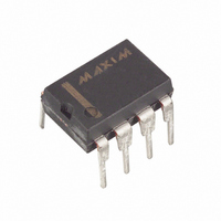
DS1302 Maxim Integrated Products, DS1302 Datasheet

DS1302
Specifications of DS1302
Available stocks
Related parts for DS1302
DS1302 Summary of contents
Page 1
... SO (208 mils) 0°C to +70° (150 mils) -40°C to +85° (150 mils TOP VIEW CC2 SCLK I GND 4 5 DIP (300 mils CC2 CC1 SCLK I/O GND (208 mils/150 mils) TOP MARK* DS1302 DS1302 DS1302S DS1302S DS1302Z DS1302ZN DS1302 CC1 REV: 120208 ...
Page 2
... CE, I/O (data line), and SCLK (serial clock). Data can be transferred to and from the clock/RAM 1 byte at a time burst bytes. The DS1302 is designed to operate on very low power and retain data and clock information on less than 1μW. ...
Page 3
... CONTROL LOGIC SCLK TYPICAL OPERATING CHARACTERISTICS (V = 3.3V +25°C, unless otherwise noted vs. V CC1T CC1T 400 350 300 250 200 150 100 2.0 3.0 V (V) CC1 X2 X1 DS1302 1Hz REAL TIME CLOCK COMMAND AND RAM 4.0 5 vs. V CC2T CC2T 2.0 3.0 4.0 5 ...
Page 4
... For more information on crystal selection and crystal layout considerations, refer to Application Note 58: Crystal Considerations for Dallas Real-Time Clocks. The DS1302 can also be driven by an external 32.768kHz oscillator. In this 3 X2 configuration, the X1 pin is connected to the external oscillator signal and the X2 pin is floated ...
Page 5
... Figure 3 shows the command byte. A command byte initiates each data transfer. The MSB (bit 7) must be a logic writes to the DS1302 will be disabled. Bit 6 specifies clock/calendar data if logic 0 or RAM data if logic 1. Bits specify the designated registers to be input or output, and the LSB (bit 0) specifies a write operation (input) if logic 0 or read operation (output) if logic 1 ...
Page 6
... CE. To avoid rollover issues, once the countdown chain is reset, the remaining time and date registers must be written within 1 second. The DS1302 can be run in either 12-hour or 24-hour mode. Bit 7 of the hours register is defined as the 12- or 24- hour mode-select bit. When high, the 12-hour mode is selected. In the 12-hour mode, bit 5 is the AM/ PM bit with logic high being PM. In the 24-hour mode, bit 5 is the second 10-hour bit (20– ...
Page 7
... Bit 7 of the seconds register is defined as the clock halt (CH) flag. When this bit is set to logic 1, the clock oscillator is stopped and the DS1302 is placed into a low-power standby mode with a current drain of less than 100nA. When this bit is written to logic 0, the clock will start. The initial power-on state is not defined. ...
Page 8
... REGISTER SUMMARY A register data format summary is shown in Table 3. CRYSTAL SELECTION A 32.768kHz crystal can be directly connected to the DS1302 via pins 2 and 3 (X1, X2). The crystal selected for use should have a specified load capacitance (C layout consideration, refer to Application Note 58: Crystal Considerations for Dallas Real-Time Clocks. ...
Page 9
Table 3. Register Address/Definition RTC READ WRITE BIT 7 BIT 6 81h 80h CH 83h 82h 12/ 24 85h 84h 0 87h 86h 0 0 89h 88h 0 0 8Bh 8Ah 0 0 8Dh 8Ch 8Fh 8Eh WP 0 91h ...
Page 10
ABSOLUTE MAXIMUM RATINGS Voltage Range on Any Pin Relative to Ground……………………………………………………………….-0.5Vto +7.0V Operating Temperature Range, Commercial………………………………………………………………….0°C to +70°C Operating Temperature Range, Industrial (IND)……………………………………………………………-40°C to +85°C Storage Temperature Range……………………………………………………………………………..….-55°C to +125°C Soldering Temperature (leads, 10 seconds)………………………………………………………………..………….260°C Soldering Temperature (surface mount)………………………………………………..…….See IPC/JEDEC ...
Page 11
CAPACITANCE (T = +25°C) A PARAMETER SYMBOL Input Capacitance C I/O Capacitance C AC ELECTRICAL CHARACTERISTICS (T = 0°C to +70° -40°C to +85°C.) (Note PARAMETER Data to CLK Setup CLK to Data Hold ...
Page 12
Figure 6. Timing Diagram: Read Data Transfer SCLK CDH t DC I/O ADDRESS/COMMAND BYTE Figure 7. Timing Diagram: Write Data Transfer SCLK CDH t ...
Page 13
... No circuit patent licenses are implied. Maxim/Dallas Semiconductor reserves the right to change the circuitry and specifications without notice at any time The Maxim logo is a registered trademark of Maxim Integrated Products, Inc. The Dallas logo is a registered trademark of Dallas Semiconductor Corporation. DS1302 Trickle-Charge Timekeeping Chip DESCRIPTION © ...


