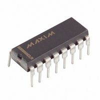
DS1306 Maxim Integrated Products, DS1306 Datasheet - Page 12

DS1306
Manufacturer Part Number
DS1306
Description
IC RTC SERIAL ALARM 16-DIP
Manufacturer
Maxim Integrated Products
Type
Clock/Calendar/Alarmr
Datasheet
1.DS1306E.pdf
(22 pages)
Specifications of DS1306
Memory Size
96B
Time Format
HH:MM:SS (12/24 hr)
Date Format
YY-MM-DD-dd
Interface
SPI, 3-Wire Serial
Voltage - Supply
2 V ~ 5.5 V
Operating Temperature
0°C ~ 70°C
Mounting Type
Through Hole
Package / Case
16-DIP (0.300", 7.62mm)
Lead Free Status / RoHS Status
Contains lead / RoHS non-compliant
Available stocks
Company
Part Number
Manufacturer
Quantity
Price
Part Number:
DS1306
Manufacturer:
DALLAS
Quantity:
20 000
Company:
Part Number:
DS1306+
Manufacturer:
Maxim
Quantity:
2 827
Part Number:
DS1306E
Manufacturer:
MAXIM/美信
Quantity:
20 000
Company:
Part Number:
DS1306E+
Manufacturer:
Maxim
Quantity:
5 860
Company:
Part Number:
DS1306E+T&R
Manufacturer:
MAXIM
Quantity:
3
Company:
Part Number:
DS1306E+TR
Manufacturer:
MICROCHIP
Quantity:
19 220
Part Number:
DS1306E+TR
Manufacturer:
MAXIM/美信
Quantity:
20 000
Part Number:
DS1306EN
Manufacturer:
MAXIM/美信
Quantity:
20 000
Company:
Part Number:
DS1306EN+
Manufacturer:
Maxim
Quantity:
3 844
Part Number:
DS1306EN+
Manufacturer:
MAXIM/美信
Quantity:
20 000
ADDRESS AND DATA BYTES
Address and data bytes are shifted MSB first into the serial data input (SDI) and out of the serial data
output (SDO). Any transfer requires the address of the byte to specify a write or read to either a RTC or
RAM location, followed by one or more bytes of data. Data is transferred out of the SDO for a read
operation and into the SDI for a write operation (Figures 6 and 7).
Figure 6. SPI SINGLE-BYTE WRITE
Figure 7. SPI SINGLE-BYTE READ
The address byte is always the first byte entered after CE is driven high. The most significant bit (A7) of
this byte determines if a read or write takes place. If A7 is 0, one or more read cycles occur. If A7 is 1,
one or more write cycles occur.
Data transfers can occur one byte at a time or in multiple-byte burst mode. After CE is driven high an
address is written to the DS1306. After the address, 1 or more data bytes can be written or read. For a
single-byte transfer, one byte is read or written and then CE is driven low. For a multiple-byte transfer,
however, multiple bytes can be read or written to the DS1306 after the address has been written. Each
read or write cycle causes the RTC register or RAM address to automatically increment. Incrementing
continues until the device is disabled. When the RTC is selected, the address wraps to 00h after
incrementing to 1Fh (during a read) and wraps to 80h after incrementing to 9Fh (during a write). When
the RAM is selected, the address wraps to 20h after incrementing to 7Fh (during a read) and wraps to
A0h after incrementing to FFh (during a write).
* SCLK CAN BE EITHER POLARITY.
* SCLK CAN BE EITHER POLARITY.
SERMODE = V
SERMODE = V
CC
CC
12 of 22


