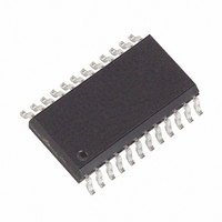
DS17885SN-3+ Maxim Integrated Products, DS17885SN-3+ Datasheet - Page 27

DS17885SN-3+
Manufacturer Part Number
DS17885SN-3+
Description
IC RTC 3V 8K NV RAM 24SOIC
Manufacturer
Maxim Integrated Products
Type
Clock/Calendar/NVSRAMr
Datasheet
1.DS17285S-5.pdf
(31 pages)
Specifications of DS17885SN-3+
Memory Size
64K (8K x 8)
Time Format
HH:MM:SS (12/24 hr)
Date Format
YY-MM-DD-dd
Interface
Parallel
Voltage - Supply
2.7 V ~ 3.7 V
Operating Temperature
-40°C ~ 85°C
Mounting Type
Surface Mount
Package / Case
24-SOIC (7.5mm Width)
Lead Free Status / RoHS Status
Lead free / RoHS Compliant
An SMI recovery register stack is located in the extend-
ed register bank, locations 4Eh and 4Fh. This register
stack, shown below, can be used by the BIOS to recov-
er from an SMI occurring during an RTC read or write.
The RTC address is latched on the falling edge of the
ALE signal. Each time an RTC address is latched, the
register address stack is pushed. The stack is only four
registers deep, holding the three previous RTC
addresses in addition to the current RTC address being
accessed. Figure 8 illustrates how the BIOS could
recover the RTC address when an SMI occurs.
Figure 8. ALE Waveform
ALE
DV0
System Maintenance Interrupt
7
AD6
(SMI) Recovery Stack
6
AD5
1
5
____________________________________________________________________
4Eh RTC ADDRESS-2
4Fh RTC ADDRESS-3
2
REGISTER BIT DEFINITION
RTC ADDRESS
RTC ADDRESS-1
SMI Recovery Stack
AD4
4
1) The RTC address is latched.
2) An SMI is generated before an RTC read or write
3
4) RTC address 4Eh is latched and the address from 1
AD3
3
occurs.
RTC address 0Ah is latched and the address from 1
is pushed to the “RTC Address–1” stack location.
This step is necessary to change the bank select bit,
DV0 = 1.
is pushed to location 4Eh, “RTC Address–2” while
0Ah is pushed to the “RTC Address–1” location. The
data in this register, 4Eh, is the RTC address lost due
to the SMI.
3
Real-Time Clocks
AD2
2
AD1
1
4
AD0
0
27


