DS1743W-150+ Maxim Integrated Products, DS1743W-150+ Datasheet - Page 6
DS1743W-150+
Manufacturer Part Number
DS1743W-150+
Description
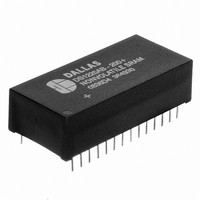
IC RTC RAM Y2K 3.3V 120NS 28EDIP
Manufacturer
Maxim Integrated Products
Type
Clock/Calendar/NVSRAM/Y2Kr
Datasheet
1.DS1743W-120.pdf
(16 pages)
Specifications of DS1743W-150+
Memory Size
64K (8K x 8)
Time Format
HH:MM:SS (24 hr)
Date Format
YY-MM-DD-dd
Interface
Parallel
Voltage - Supply
3 V ~ 3.6 V
Operating Temperature
0°C ~ 70°C
Mounting Type
Through Hole
Package / Case
28-DIP Module (600 mil), 28-EDIP
Function
Clock/Calendar/NV Timekeeping RAM
Rtc Memory Size
8192 Byte
Supply Voltage (max)
3.63 V
Supply Voltage (min)
2.97 V
Maximum Operating Temperature
+ 70 C
Minimum Operating Temperature
0 C
Mounting Style
Through Hole
Rtc Bus Interface
Parallel
Supply Current
15 mA
Lead Free Status / RoHS Status
Lead free / RoHS Compliant


CLOCK ACCURACY (DIP MODULE)
The DS1743 is guaranteed to keep time accuracy to within 1 minute per month at +25C. The RTC is
calibrated at the factory by Dallas Semiconductor using nonvolatile tuning elements, and does not require
additional calibration. For this reason, methods of field clock calibration are not available and not
necessary. The electrical environment also affects clock accuracy, so caution should be taken to place the
RTC in the lowest-level EMI section of the PC board layout. For additional information, please refer to
Application Note 58: Crystal Considerations with Dallas Real-Time Clocks.
CLOCK ACCURACY (PowerCap MODULE)
The DS1743 and DS9034PCX are each individually tested for accuracy. Once mounted together, the
module will typically keep time accuracy to within 1.53 minutes per month (35ppm) at +25°C. The
electrical environment also affects clock accuracy, so caution should be taken to place the RTC in the
lowest-level EMI section of the PC board layout. For additional information, please refer to Application
Note 58: Crystal Considerations with Dallas Real-Time Clocks.
Table 2. Register Map
RETRIEVING DATA FROM RAM OR CLOCK
The DS1743 is in the read mode whenever OE (output enable) is low, WE (write enable) is high, and CE
(chip enable) is low. The device architecture allows ripple-through access to any of the address locations in
the NV SRAM. Valid data will be available at the DQ pins within t
providing that the, CE and OE access times and states are satisfied. If CE, or OE access times and states
are not met, valid data will be available at the latter of chip enable access (t
time (t
activated before t
changed while CE and OE remain valid, output data will remain valid for output data hold time (t
will then go indeterminate until the next address access.
ADDRESS
OSC = STOP BIT
W = WRITE BIT
Note: All indicated “X” bits must be set to “0” when written to ensure proper clock operation.
1FFD
1FFA
1FFE
1FFC
1FFB
1FFF
1FF9
1FF8
CEA
). The state of the data input/output pins (DQ) is controlled by CE and OE. If the outputs are
OSC
BF
B
W
X
X
X
X
7
AA
R = READ BIT
X = SEE NOTE BELOW
, the data lines are driven to an intermediate state until t
FT
B
X
X
X
R
6
10 Year
10 Minutes
10 Seconds
B
X
X
10 Century
5
10 Hour
10 Date
Month
DATA
B
10
X
FT = FREQUENCY TEST
BF = BATTERY FLAG
4
DS1743/DS1743P Y2K-Compliant, Nonvolatile Timekeeping RAMs
B
X
3
6 of 16
Seconds
Minutes
Century
B
Month
Hour
Year
Date
2
Day
B
1
AA
B
after the last address input is stable,
0
CEA
FUNCTION
AA
Minutes
Seconds
Control
) or at output enable access
Month
Hour
Year
Date
. If the address inputs are
Day
RANGE
00–99
01–12
01–31
01–07
00–23
00–59
00–59
00–39
OH
) but
Related parts for DS1743W-150+
Image
Part Number
Description
Manufacturer
Datasheet
Request
R

Part Number:
Description:
IC RTC RAM Y2K 3.3V 120NS 28EDIP
Manufacturer:
Maxim Integrated Products
Datasheet:
Part Number:
Description:
IC RTC RAM Y2K 3.3V 120NS 28EDIP
Manufacturer:
Maxim Integrated Products
Datasheet:
Part Number:
Description:
IC RTC RAM Y2K 3.3V 120NS 28EDIP
Manufacturer:
Maxim Integrated Products
Datasheet:

Part Number:
Description:
Real Time Clock
Manufacturer:
Maxim Integrated Products
Datasheet:
Part Number:
Description:
Real Time Clock
Manufacturer:
Maxim Integrated Products
Datasheet:
Part Number:
Description:
MAX7528KCWPMaxim Integrated Products [CMOS Dual 8-Bit Buffered Multiplying DACs]
Manufacturer:
Maxim Integrated Products
Datasheet:
Part Number:
Description:
Single +5V, fully integrated, 1.25Gbps laser diode driver.
Manufacturer:
Maxim Integrated Products
Datasheet:
Part Number:
Description:
Single +5V, fully integrated, 155Mbps laser diode driver.
Manufacturer:
Maxim Integrated Products
Datasheet:
Part Number:
Description:
VRD11/VRD10, K8 Rev F 2/3/4-Phase PWM Controllers with Integrated Dual MOSFET Drivers
Manufacturer:
Maxim Integrated Products
Datasheet:
Part Number:
Description:
Highly Integrated Level 2 SMBus Battery Chargers
Manufacturer:
Maxim Integrated Products
Datasheet:
Part Number:
Description:
Current Monitor and Accumulator with Integrated Sense Resistor; ; Temperature Range: -40°C to +85°C
Manufacturer:
Maxim Integrated Products
Part Number:
Description:
TSSOP 14/A�/RS-485 Transceivers with Integrated 100O/120O Termination Resis
Manufacturer:
Maxim Integrated Products
Part Number:
Description:
TSSOP 14/A�/RS-485 Transceivers with Integrated 100O/120O Termination Resis
Manufacturer:
Maxim Integrated Products
Part Number:
Description:
QFN 16/A�/AC-DC and DC-DC Peak-Current-Mode Converters with Integrated Step
Manufacturer:
Maxim Integrated Products
Part Number:
Description:
TDFN/A/65V, 1A, 600KHZ, SYNCHRONOUS STEP-DOWN REGULATOR WITH INTEGRATED SWI
Manufacturer:
Maxim Integrated Products